- 您現(xiàn)在的位置:買賣IC網(wǎng) > PDF目錄300038 > TMS570LS10216ASZWTQR (TEXAS INSTRUMENTS INC) 32-BIT, FLASH, 160 MHz, RISC MICROCONTROLLER, PBGA337 PDF資料下載
參數(shù)資料
| 型號: | TMS570LS10216ASZWTQR |
| 廠商: | TEXAS INSTRUMENTS INC |
| 元件分類: | 微控制器/微處理器 |
| 英文描述: | 32-BIT, FLASH, 160 MHz, RISC MICROCONTROLLER, PBGA337 |
| 封裝: | GERRN, PLASTIC, NFBGA-337 |
| 文件頁數(shù): | 65/102頁 |
| 文件大小: | 1146K |
| 代理商: | TMS570LS10216ASZWTQR |
第1頁第2頁第3頁第4頁第5頁第6頁第7頁第8頁第9頁第10頁第11頁第12頁第13頁第14頁第15頁第16頁第17頁第18頁第19頁第20頁第21頁第22頁第23頁第24頁第25頁第26頁第27頁第28頁第29頁第30頁第31頁第32頁第33頁第34頁第35頁第36頁第37頁第38頁第39頁第40頁第41頁第42頁第43頁第44頁第45頁第46頁第47頁第48頁第49頁第50頁第51頁第52頁第53頁第54頁第55頁第56頁第57頁第58頁第59頁第60頁第61頁第62頁第63頁第64頁當(dāng)前第65頁第66頁第67頁第68頁第69頁第70頁第71頁第72頁第73頁第74頁第75頁第76頁第77頁第78頁第79頁第80頁第81頁第82頁第83頁第84頁第85頁第86頁第87頁第88頁第89頁第90頁第91頁第92頁第93頁第94頁第95頁第96頁第97頁第98頁第99頁第100頁第101頁第102頁
PRODUCTPREVIEW
www.ti.com
SPNS141D – AUGUST 2010 – REVISED JANUARY 2011
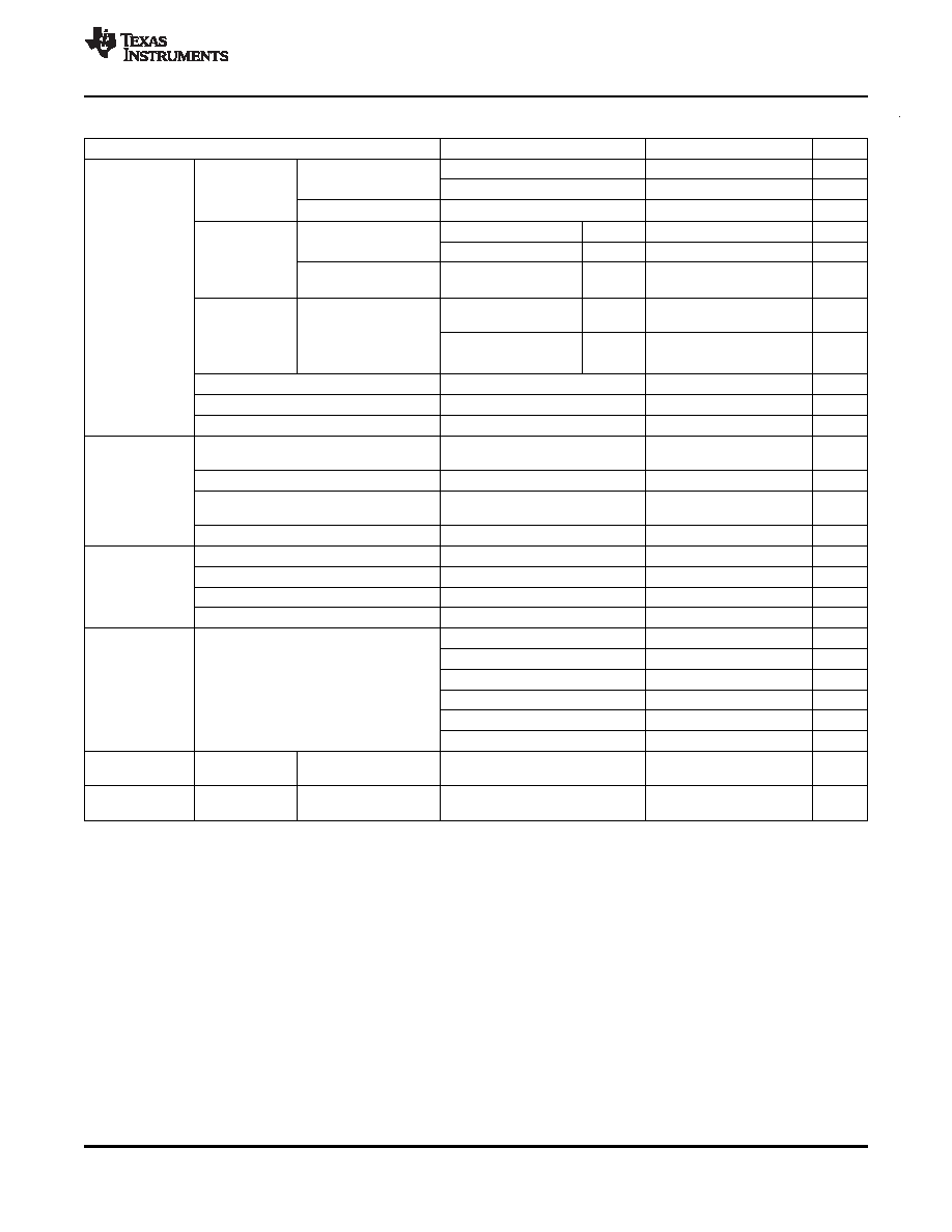
Electrical Characteristics Over Operating Free-Air Temperature Range (continued)
Parameter
Test Conditions
MIN
TYP
MAX
Unit
ICC
(3)
VCC Digital
All packages
HCLK = 100MHz, VCLK = 100MHz
350
mA
supply current
HCLK = 140MHz, VCLK= 70MHz
390
mA
(Operating
BGA packages
HCLK = 160MHz, VCLK = 80MHz
430
mA
mode)
VCC Digital
All packages
STCCLK = 46.666MHz
Peak
510
mA
supply current
STCCLK = 50.0MHz
Peak
540
mA
(CPU selftest
BGA packages
STCCLK = 53.333MHz
Peak
580
mA
mode:
LBIST)(4)(5)
VCC Digital
All packages
HCLK=80MHz,
Peak
340
mA
supply current
VCLK=40MHz
(Mem selftest
HCLK=100MHz,
Peak
430
mA
mode:
VLCK=100MHz
PBIST)(4)(6)
VCC Digital supply current (doze mode)
OSCIN = 6 MHz, VCC = 1.65 V
(7)
35
mA
VCC Digital supply current (snooze mode)
All frequencies, VCC = 1.65 V
(7)
30
mA
VCC Digital supply current (sleep mode)
All frequencies, VCC = 1.65 V
(7)
25
mA
ICCIO
VCCIO Digital supply current (operating
No DC load, VCCIO = 3.6 V
(8)
15
mA
mode)
VCCIO Digital supply current (doze mode)
No DC load, VCCIO = 3.6 V
(8)
700
A
VCCIO Digital supply current (snooze
No DC load, VCCIO = 3.6 V
(8)
100
A
mode)
VCCIO Digital supply current (sleep mode)
No DC load, VCCIO = 3.6 V
(8)
100
A
ICCAD
VCCAD supply current (operating mode)
All frequencies, VCCAD = 3.6 V
30
mA
VCCAD supply current (doze mode)
All frequencies, VCCAD = 3.6 V
(7)
200
A
VCCAD supply current (snooze mode)
All frequencies, VCCAD = 3.6 V
(7)
200
A
VCCAD supply current (sleep mode)
All frequencies, VCCAD = 3.6 V
(7)
200
A
ICCP
VCCP pump supply current
VCCP = 3.6 V read operation
25
mA
VCCP = 3.6 V program
(9)
90
mA
VCCP = 3.6 V erase
90
mA
VCCP = 3.6 V doze mode
(10)
5
A
VCCP = 3.6 V snooze mode
(10)
5
A
VCCP = 3.6 V sleep mode
(10)
5
A
CI
Input
2
pF
capacitance(11)
CO
Output
3
pF
capacitance
(3)
Typical values are at Vcc=1.5V and maximum values are at Vcc=1.65V
(4)
The peak current is measured on the TI EVM board with two 10F and thirteen 100nF capacitors on VCC domain. Running at a lower
frequency consumes less current.
(5)
LBIST currents specified are for execution of LBIST with a certain STC clock. Lower current consumption can be achieved by
configuring a slower STC Clock frequency. The current peak duration can last for the duration of 1 LBIST test interval.
(6)
PBIST currents specified are for execution of PBIST on all RAMs(Group 1- 14) and all the algrithms. Lower current consumption can be
achieved by configuring a slower HCLK frequency. Different algorithms consume different current. For more information, please refer to
Basic PBIST Configuration and influence on current consumption (SPNA128).
(7)
For Flash banks/pumps in sleep mode.
(8)
I/O pins configured as inputs or outputs with no load. All pulldown inputs
≤ 0.2 V. All pullup inputs ≥ VCCIO - 0.2 V.
(9)
This assumes reading from one bank while programming a different bank.
(10) For Flash banks/pumps in sleep mode.
(11) The maximum input capacitance CI of the FlexRay RX pin(s) is 10pF.
Copyright 2010–2011, Texas Instruments Incorporated
Device Electrical Specifications
65
相關(guān)PDF資料 |
PDF描述 |
|---|---|
| TMX320DM642GNZ500 | 64-BIT, 75.19 MHz, OTHER DSP, PBGA548 |
| TN4002PM | 10 MHz - 500 MHz RF/MICROWAVE WIDE BAND LOW POWER AMPLIFIER |
| TN5171PM | 20 MHz - 150 MHz RF/MICROWAVE WIDE BAND MEDIUM POWER AMPLIFIER |
| TOCP172-1MB | 970/1000 um, MULTI MODE, SIMPLEX FIBER OPTIC CONNECTOR |
| TOCP172-20CB | 970/1000 um, MULTI MODE, SIMPLEX FIBER OPTIC CONNECTOR |
相關(guān)代理商/技術(shù)參數(shù) |
參數(shù)描述 |
|---|---|
| TMS570LS10216SPGE | 制造商:Texas Instruments 功能描述: |
| TMS570LS20206 | 制造商:TI 制造商全稱:Texas Instruments 功能描述:16/32-BIT RISC Flash Microcontroller |
| TMS570LS20206-EP | 制造商:TI 制造商全稱:Texas Instruments 功能描述:TMS570LS Series 16/32-BIT RISC Flash Microcontroller |
| TMS570LS20216 | 制造商:TI 制造商全稱:Texas Instruments 功能描述:16/32-BIT RISC Flash Microcontroller |
| TMS570LS31 | 制造商:TI 制造商全稱:Texas Instruments 功能描述:TMS570LS31 Hercules ARM Safety MCU Development Kit (HDK) |
發(fā)布緊急采購,3分鐘左右您將得到回復(fù)。