- 您現(xiàn)在的位置:買賣IC網(wǎng) > PDF目錄383961 > TMX320DM6437BZWTA (Texas Instruments, Inc.) Digital Media Processor PDF資料下載
參數(shù)資料
| 型號: | TMX320DM6437BZWTA |
| 廠商: | Texas Instruments, Inc. |
| 英文描述: | Digital Media Processor |
| 中文描述: | 數(shù)字媒體處理器 |
| 文件頁數(shù): | 33/309頁 |
| 文件大小: | 2216K |
| 代理商: | TMX320DM6437BZWTA |
第1頁第2頁第3頁第4頁第5頁第6頁第7頁第8頁第9頁第10頁第11頁第12頁第13頁第14頁第15頁第16頁第17頁第18頁第19頁第20頁第21頁第22頁第23頁第24頁第25頁第26頁第27頁第28頁第29頁第30頁第31頁第32頁當(dāng)前第33頁第34頁第35頁第36頁第37頁第38頁第39頁第40頁第41頁第42頁第43頁第44頁第45頁第46頁第47頁第48頁第49頁第50頁第51頁第52頁第53頁第54頁第55頁第56頁第57頁第58頁第59頁第60頁第61頁第62頁第63頁第64頁第65頁第66頁第67頁第68頁第69頁第70頁第71頁第72頁第73頁第74頁第75頁第76頁第77頁第78頁第79頁第80頁第81頁第82頁第83頁第84頁第85頁第86頁第87頁第88頁第89頁第90頁第91頁第92頁第93頁第94頁第95頁第96頁第97頁第98頁第99頁第100頁第101頁第102頁第103頁第104頁第105頁第106頁第107頁第108頁第109頁第110頁第111頁第112頁第113頁第114頁第115頁第116頁第117頁第118頁第119頁第120頁第121頁第122頁第123頁第124頁第125頁第126頁第127頁第128頁第129頁第130頁第131頁第132頁第133頁第134頁第135頁第136頁第137頁第138頁第139頁第140頁第141頁第142頁第143頁第144頁第145頁第146頁第147頁第148頁第149頁第150頁第151頁第152頁第153頁第154頁第155頁第156頁第157頁第158頁第159頁第160頁第161頁第162頁第163頁第164頁第165頁第166頁第167頁第168頁第169頁第170頁第171頁第172頁第173頁第174頁第175頁第176頁第177頁第178頁第179頁第180頁第181頁第182頁第183頁第184頁第185頁第186頁第187頁第188頁第189頁第190頁第191頁第192頁第193頁第194頁第195頁第196頁第197頁第198頁第199頁第200頁第201頁第202頁第203頁第204頁第205頁第206頁第207頁第208頁第209頁第210頁第211頁第212頁第213頁第214頁第215頁第216頁第217頁第218頁第219頁第220頁第221頁第222頁第223頁第224頁第225頁第226頁第227頁第228頁第229頁第230頁第231頁第232頁第233頁第234頁第235頁第236頁第237頁第238頁第239頁第240頁第241頁第242頁第243頁第244頁第245頁第246頁第247頁第248頁第249頁第250頁第251頁第252頁第253頁第254頁第255頁第256頁第257頁第258頁第259頁第260頁第261頁第262頁第263頁第264頁第265頁第266頁第267頁第268頁第269頁第270頁第271頁第272頁第273頁第274頁第275頁第276頁第277頁第278頁第279頁第280頁第281頁第282頁第283頁第284頁第285頁第286頁第287頁第288頁第289頁第290頁第291頁第292頁第293頁第294頁第295頁第296頁第297頁第298頁第299頁第300頁第301頁第302頁第303頁第304頁第305頁第306頁第307頁第308頁第309頁
www.ti.com
P
TMS320DM6437
Digital Media Processor
SPRS345B–NOVEMBER 2006–REVISED MARCH 2007
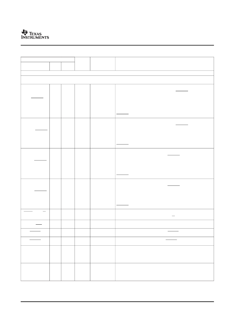
Table 2-10. EMIFA Terminal Functions (EMIFA Pinout Mode 1, AEM[2:0] = 001)
SIGNAL
TYPE
(1)
OTHER
(2)(3)
DESCRIPTION
ZWT
NO.
EMIFA FUNCTIONAL PINS: 8-Bit ASYNC/NOR (EMIFA Pinout Mode 1, AEM[2:0] = 001)
Actual pin functions are determined by the PINMUX0 and PINMUX1 register bit settings (e.g., PCIEN, AEAW[2:0], AEM[2:0], etc.). For
more details, see
Section 3.7
,
Multiplexed Pin Configurations
.
ZDU
NO.
NAME
This pin is multiplexed between VPBE (VENC), EMIFA, and GPIO.
For EMIFA, this pin is Chip Select 2 output EM_CS2 for use with
asynchronous memories (i.e., NOR flash).
This is the chip select for the default boot and ROM boot modes.
G0/EM_CS2/
GP[12]
IPD
DV
DD33
C19
C22
I/O/Z
Note:
This pin features an internal pulldown (IPD). If this pin is
connected and used as an EMIFA chip select signal, for proper device
operation, an external pullup resistor
must
be used to ensure the
EM_CSx function defaults to an inactive (high) state.
This pin is multiplexed between VPBE (VENC), EMIFA, and GPIO.
For EMIFA, this pin is Chip Select 3 output EM_CS3 for use with
asynchronous memories (i.e., NOR flash).
LCD_OE/EM_CS3/
GP[13]
IPD
DV
DD33
C18
D22
I/O/Z
Note:
This pin features an internal pulldown (IPD). If this pin is
connected and used as an EMIFA chip select signal, for proper device
operation, an external pullup resistor
must
be used to ensure the
EM_CSx function defaults to an inactive (high) state.
This pin is multiplexed between VPBE (VENC), EMIFA, and GPIO.
For EMIFA, it is Chip Select 4 output EM_CS4 for use with
asynchronous memories (i.e., NOR flash).
VSYNC/EM_CS4/
GP[32]
IPD
DV
DD33
E19
H22
I/O/Z
Note:
This pin features an internal pulldown (IPD). If this pin is
connected and used as an EMIFA chip select signal, for proper device
operation, an external pullup resistor
must
be used to ensure the
EM_CSx function defaults to an inactive (high) state.
This pin is multiplexed between VPBE (VENC), EMIFA, and GPIO.
For EMIFA, it is Chip Select 5 output EM_CS5 for use with
asynchronous memories (i.e., NOR flash).
HSYNC/EM_CS5/
GP[33]
IPD
DV
DD33
F19
J22
I/O/Z
Note:
This pin features an internal pulldown (IPD). If this pin is
connected and used as an EMIFA chip select signal, for proper device
operation, an external pullup resistor
must
be used to ensure the
EM_CSx function defaults to an inactive (high) state.
This pin is multiplexed between VPFE (CCDC), EMIFA, and GPIO.
C_WE/EM_R/W/
GP[35]
IPD
DV
DD33
D13
C17
I/O/Z
For EMIFA, it is read/write output EM_R/W.
For EMIFA (ASYNC/NOR), this pin is wait state extension input
EM_WAIT.
EM_WAIT/
(RDY/BSY)
IPU
DV
DD33
IPU
DV
DD33
IPU
DV
DD33
E15
D20
I/O/Z
EM_OE
D15
D19
I/O/Z
For EMIFA, it is output enable output EM_OE.
EM_WE
E14
C19
I/O/Z
For EMIFA, it is write enable output EM_WE.
This pin is multiplexed between VPBE (VENC), EMIFA, and GPIO.
R2/EM_BA[0]/
GP[6]/(AEM1)
IPD
DV
DD33
For EMIFA, this is the Bank Address 0 output (EM_BA[0]). When
connected to an 8-bit asynchronous memory, this pin is the lowest
order bit of the byte address.
This pin is multiplexed between VPBE (VENC), EMIFA, and GPIO.
C17
E20
I/O/Z
B2/EM_BA[1]/
GP[5]/(AEM0)
IPD
DV
DD33
For EMIFA, this is the Bank Address 1 output EM_BA[1]. When
connected to an 8-bit asynchronous memory, this pin is the 2nd bit of
the address.
C16
C20
I/O/Z
(1)
(2)
I = Input, O = Output, Z = High impedance, S = Supply voltage, GND = Ground, A = Analog signal
IPD = Internal pulldown, IPU = Internal pullup. For more detailed information on pullup/pulldown resistors and situations where external
pullup/pulldown resistors are required, see
Section 3.9.1
,
Pullup/Pulldown Resistors
.
Specifies the operating I/O supply voltage for each signal
(3)
Submit Documentation Feedback
Device Overview
33
相關(guān)PDF資料 |
PDF描述 |
|---|---|
| TMS320DM6443_07 | Digital Media System-on-Chip |
| TMX320DM6443AZWT | Digital Media System-on-Chip |
| TMX320DM6443ZWT | Digital Media System-on-Chip |
| TMS320DM647_08 | Digital Media Processor |
| TMS320DM647ZUT720 | Digital Media Processor |
相關(guān)代理商/技術(shù)參數(shù) |
參數(shù)描述 |
|---|---|
| TMX320DM6441CZWT | 制造商:Texas Instruments 功能描述: |
| TMX320DM6441DZWT | 制造商:Texas Instruments 功能描述:DAVINCI DIGITAL MEDIA SYSTEM-ON-CHIP - Tape and Reel |
| TMX320DM6443AZWT | 制造商:Rochester Electronics LLC 功能描述:DAVINCI DIGITAL MEDIA SYSTEM-ON-CHIP - Tape and Reel |
| TMX320DM6443BZWT | 制造商:Texas Instruments 功能描述: |
| TMX320DM6443CZWT | 制造商:Texas Instruments 功能描述: |
發(fā)布緊急采購,3分鐘左右您將得到回復(fù)。