- 您現(xiàn)在的位置:買賣IC網(wǎng) > PDF目錄383961 > TMX320DM6437BZWTA (Texas Instruments, Inc.) Digital Media Processor PDF資料下載
參數(shù)資料
| 型號: | TMX320DM6437BZWTA |
| 廠商: | Texas Instruments, Inc. |
| 英文描述: | Digital Media Processor |
| 中文描述: | 數(shù)字媒體處理器 |
| 文件頁數(shù): | 51/309頁 |
| 文件大小: | 2216K |
| 代理商: | TMX320DM6437BZWTA |
第1頁第2頁第3頁第4頁第5頁第6頁第7頁第8頁第9頁第10頁第11頁第12頁第13頁第14頁第15頁第16頁第17頁第18頁第19頁第20頁第21頁第22頁第23頁第24頁第25頁第26頁第27頁第28頁第29頁第30頁第31頁第32頁第33頁第34頁第35頁第36頁第37頁第38頁第39頁第40頁第41頁第42頁第43頁第44頁第45頁第46頁第47頁第48頁第49頁第50頁當前第51頁第52頁第53頁第54頁第55頁第56頁第57頁第58頁第59頁第60頁第61頁第62頁第63頁第64頁第65頁第66頁第67頁第68頁第69頁第70頁第71頁第72頁第73頁第74頁第75頁第76頁第77頁第78頁第79頁第80頁第81頁第82頁第83頁第84頁第85頁第86頁第87頁第88頁第89頁第90頁第91頁第92頁第93頁第94頁第95頁第96頁第97頁第98頁第99頁第100頁第101頁第102頁第103頁第104頁第105頁第106頁第107頁第108頁第109頁第110頁第111頁第112頁第113頁第114頁第115頁第116頁第117頁第118頁第119頁第120頁第121頁第122頁第123頁第124頁第125頁第126頁第127頁第128頁第129頁第130頁第131頁第132頁第133頁第134頁第135頁第136頁第137頁第138頁第139頁第140頁第141頁第142頁第143頁第144頁第145頁第146頁第147頁第148頁第149頁第150頁第151頁第152頁第153頁第154頁第155頁第156頁第157頁第158頁第159頁第160頁第161頁第162頁第163頁第164頁第165頁第166頁第167頁第168頁第169頁第170頁第171頁第172頁第173頁第174頁第175頁第176頁第177頁第178頁第179頁第180頁第181頁第182頁第183頁第184頁第185頁第186頁第187頁第188頁第189頁第190頁第191頁第192頁第193頁第194頁第195頁第196頁第197頁第198頁第199頁第200頁第201頁第202頁第203頁第204頁第205頁第206頁第207頁第208頁第209頁第210頁第211頁第212頁第213頁第214頁第215頁第216頁第217頁第218頁第219頁第220頁第221頁第222頁第223頁第224頁第225頁第226頁第227頁第228頁第229頁第230頁第231頁第232頁第233頁第234頁第235頁第236頁第237頁第238頁第239頁第240頁第241頁第242頁第243頁第244頁第245頁第246頁第247頁第248頁第249頁第250頁第251頁第252頁第253頁第254頁第255頁第256頁第257頁第258頁第259頁第260頁第261頁第262頁第263頁第264頁第265頁第266頁第267頁第268頁第269頁第270頁第271頁第272頁第273頁第274頁第275頁第276頁第277頁第278頁第279頁第280頁第281頁第282頁第283頁第284頁第285頁第286頁第287頁第288頁第289頁第290頁第291頁第292頁第293頁第294頁第295頁第296頁第297頁第298頁第299頁第300頁第301頁第302頁第303頁第304頁第305頁第306頁第307頁第308頁第309頁
www.ti.com
P
TMS320DM6437
Digital Media Processor
SPRS345B–NOVEMBER 2006–REVISED MARCH 2007
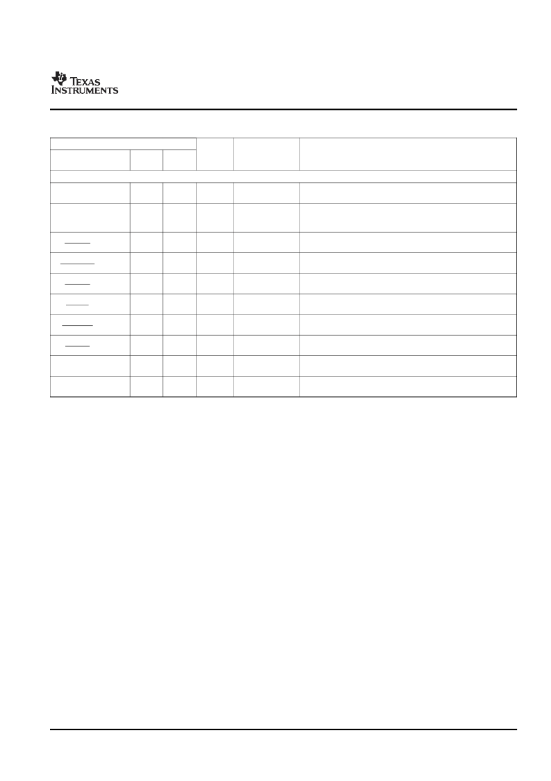
Table 2-17. VLYNQ Terminal Functions
SIGNAL
TYPE
(1)
OTHER
(2)(3)
DESCRIPTION
ZWT
NO.
ZDU
NO.
NAME
VLYNQ
IPU
DV
DD33
VLYNQ_CLOCK/
PCICLK/GP[57]
This pin is multiplexed between VLYNQ, PCI, and GPIO.
For VLYNQ, it is the clock VLYNQ_CLOCK (I/O/Z).
This pin is multiplexed between HPI, VLYNQ, PCI, and GPIO.
For VLYNQ, it is the Serial Clock run request VLYNQ_SCRUN
(I/O/Z).
This pin is multiplexed between HPI, VLYNQ, PCI, and GPIO.
For VLYNQ, it is transmit bus bit 3 output VLYNQ_TXD3.
This pin is multiplexed between HPI, VLYNQ, PCI, and GPIO.
For VLYNQ, it is transmit bus bit 2 output VLYNQ_TXD2.
This pin is multiplexed between HPI, VLYNQ, PCI, and GPIO.
For VLYNQ, it is transmit bus bit 1 output VLYNQ_TXD1.
This pin is multiplexed between HPI, VLYNQ, PCI, and GPIO.
For VLYNQ, it is transmit bus bit 0 output VLYNQ_TXD0.
This pin is multiplexed between HPI, VLYNQ, PCI, and GPIO.
For VLYNQ, it is receive bus bit 3 input VLYNQ_RXD3.
This pin is multiplexed between HPI, VLYNQ, PCI, and GPIO.
For VLYNQ, it is receive bus bit 2 input VLYNQ_RXD2.
This pin is multiplexed between HPI, VLYNQ, PCI, and GPIO.
For VLYNQ, it is receive bus bit 1 input VLYNQ_RXD1.
This pin is multiplexed between HPI, VLYNQ, PCI, and GPIO.
For VLYNQ, it is receive bus bit 0 input VLYNQ_RXD0.
A7
A8
I/O/Z
HD0/VLYNQ_SCRUN/
AD18/GP[58]
IPU
DV
DD33
C8
B9
I/O/Z
HD8/VLYNQ_TXD3/
PPERR/GP[66]
HD7/VLYNQ_TXD2/
PDEVSEL/GP[65]
HD6/VLYNQ_TXD1/
PTRDY/GP[64]
HD5/VLYNQ_TXD0/
PIRDY/GP[63]
HD4/VLYNQ_RXD3/
PFRAME/GP[62]
HD3/VLYNQ_RXD2/
PCBE2/GP[61]
HD2/VLYNQ_RXD1/
AD17/GP[60]
HD1/VLYNQ_RXD0/
AD16/GP[59]
IPD
DV
DD33
IPD
DV
DD33
IPD
DV
DD33
IPD
DV
DD33
IPD
DV
DD33
IPD
DV
DD33
IPD
DV
DD33
IPD
DV
DD33
A5
A6
I/O/Z
B6
B7
I/O/Z
D6
C7
I/O/Z
A6
A7
I/O/Z
C7
C8
I/O/Z
B7
B8
I/O/Z
A8
A9
I/O/Z
D7
C9
I/O/Z
(1)
(2)
I = Input, O = Output, Z = High impedance, S = Supply voltage, GND = Ground, A = Analog signal
IPD = Internal pulldown, IPU = Internal pullup. For more detailed information on pullup/pulldown resistors and situations where external
pullup/pulldown resistors are required, see
Section 3.9.1
,
Pullup/Pulldown Resistors
.
Specifies the operating I/O supply voltage for each signal
(3)
Submit Documentation Feedback
Device Overview
51
相關(guān)PDF資料 |
PDF描述 |
|---|---|
| TMS320DM6443_07 | Digital Media System-on-Chip |
| TMX320DM6443AZWT | Digital Media System-on-Chip |
| TMX320DM6443ZWT | Digital Media System-on-Chip |
| TMS320DM647_08 | Digital Media Processor |
| TMS320DM647ZUT720 | Digital Media Processor |
相關(guān)代理商/技術(shù)參數(shù) |
參數(shù)描述 |
|---|---|
| TMX320DM6441CZWT | 制造商:Texas Instruments 功能描述: |
| TMX320DM6441DZWT | 制造商:Texas Instruments 功能描述:DAVINCI DIGITAL MEDIA SYSTEM-ON-CHIP - Tape and Reel |
| TMX320DM6443AZWT | 制造商:Rochester Electronics LLC 功能描述:DAVINCI DIGITAL MEDIA SYSTEM-ON-CHIP - Tape and Reel |
| TMX320DM6443BZWT | 制造商:Texas Instruments 功能描述: |
| TMX320DM6443CZWT | 制造商:Texas Instruments 功能描述: |
發(fā)布緊急采購,3分鐘左右您將得到回復(fù)。