- 您現(xiàn)在的位置:買賣IC網(wǎng) > PDF目錄383961 > TMX320DM6443ZWT (Texas Instruments, Inc.) Digital Media System-on-Chip PDF資料下載
參數(shù)資料
| 型號(hào): | TMX320DM6443ZWT |
| 廠商: | Texas Instruments, Inc. |
| 英文描述: | Digital Media System-on-Chip |
| 中文描述: | 數(shù)字媒體系統(tǒng)片上 |
| 文件頁(yè)數(shù): | 43/221頁(yè) |
| 文件大小: | 1582K |
| 代理商: | TMX320DM6443ZWT |
第1頁(yè)第2頁(yè)第3頁(yè)第4頁(yè)第5頁(yè)第6頁(yè)第7頁(yè)第8頁(yè)第9頁(yè)第10頁(yè)第11頁(yè)第12頁(yè)第13頁(yè)第14頁(yè)第15頁(yè)第16頁(yè)第17頁(yè)第18頁(yè)第19頁(yè)第20頁(yè)第21頁(yè)第22頁(yè)第23頁(yè)第24頁(yè)第25頁(yè)第26頁(yè)第27頁(yè)第28頁(yè)第29頁(yè)第30頁(yè)第31頁(yè)第32頁(yè)第33頁(yè)第34頁(yè)第35頁(yè)第36頁(yè)第37頁(yè)第38頁(yè)第39頁(yè)第40頁(yè)第41頁(yè)第42頁(yè)當(dāng)前第43頁(yè)第44頁(yè)第45頁(yè)第46頁(yè)第47頁(yè)第48頁(yè)第49頁(yè)第50頁(yè)第51頁(yè)第52頁(yè)第53頁(yè)第54頁(yè)第55頁(yè)第56頁(yè)第57頁(yè)第58頁(yè)第59頁(yè)第60頁(yè)第61頁(yè)第62頁(yè)第63頁(yè)第64頁(yè)第65頁(yè)第66頁(yè)第67頁(yè)第68頁(yè)第69頁(yè)第70頁(yè)第71頁(yè)第72頁(yè)第73頁(yè)第74頁(yè)第75頁(yè)第76頁(yè)第77頁(yè)第78頁(yè)第79頁(yè)第80頁(yè)第81頁(yè)第82頁(yè)第83頁(yè)第84頁(yè)第85頁(yè)第86頁(yè)第87頁(yè)第88頁(yè)第89頁(yè)第90頁(yè)第91頁(yè)第92頁(yè)第93頁(yè)第94頁(yè)第95頁(yè)第96頁(yè)第97頁(yè)第98頁(yè)第99頁(yè)第100頁(yè)第101頁(yè)第102頁(yè)第103頁(yè)第104頁(yè)第105頁(yè)第106頁(yè)第107頁(yè)第108頁(yè)第109頁(yè)第110頁(yè)第111頁(yè)第112頁(yè)第113頁(yè)第114頁(yè)第115頁(yè)第116頁(yè)第117頁(yè)第118頁(yè)第119頁(yè)第120頁(yè)第121頁(yè)第122頁(yè)第123頁(yè)第124頁(yè)第125頁(yè)第126頁(yè)第127頁(yè)第128頁(yè)第129頁(yè)第130頁(yè)第131頁(yè)第132頁(yè)第133頁(yè)第134頁(yè)第135頁(yè)第136頁(yè)第137頁(yè)第138頁(yè)第139頁(yè)第140頁(yè)第141頁(yè)第142頁(yè)第143頁(yè)第144頁(yè)第145頁(yè)第146頁(yè)第147頁(yè)第148頁(yè)第149頁(yè)第150頁(yè)第151頁(yè)第152頁(yè)第153頁(yè)第154頁(yè)第155頁(yè)第156頁(yè)第157頁(yè)第158頁(yè)第159頁(yè)第160頁(yè)第161頁(yè)第162頁(yè)第163頁(yè)第164頁(yè)第165頁(yè)第166頁(yè)第167頁(yè)第168頁(yè)第169頁(yè)第170頁(yè)第171頁(yè)第172頁(yè)第173頁(yè)第174頁(yè)第175頁(yè)第176頁(yè)第177頁(yè)第178頁(yè)第179頁(yè)第180頁(yè)第181頁(yè)第182頁(yè)第183頁(yè)第184頁(yè)第185頁(yè)第186頁(yè)第187頁(yè)第188頁(yè)第189頁(yè)第190頁(yè)第191頁(yè)第192頁(yè)第193頁(yè)第194頁(yè)第195頁(yè)第196頁(yè)第197頁(yè)第198頁(yè)第199頁(yè)第200頁(yè)第201頁(yè)第202頁(yè)第203頁(yè)第204頁(yè)第205頁(yè)第206頁(yè)第207頁(yè)第208頁(yè)第209頁(yè)第210頁(yè)第211頁(yè)第212頁(yè)第213頁(yè)第214頁(yè)第215頁(yè)第216頁(yè)第217頁(yè)第218頁(yè)第219頁(yè)第220頁(yè)第221頁(yè)
www.ti.com
TMS320DM6443
Digital Media System-on-Chip
SPRS282E–DECEMBER 2005–REVISED MARCH 2007
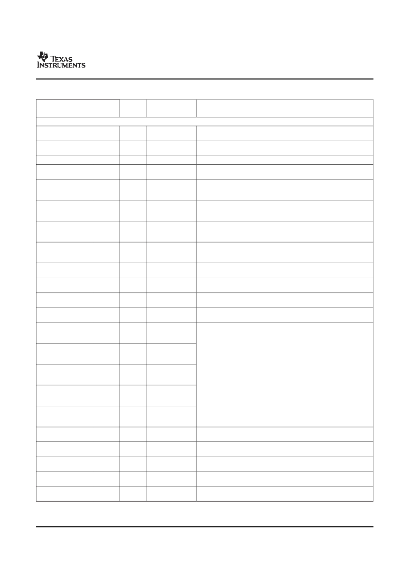
Table 2-19. VPBE Terminal Functions
SIGNAL
TYPE
(1)
OTHER
(2)(3)
DESCRIPTION
NAME
NO.
VIDEO OUT (VPBE)
IPD
DV
DD18
IPD
DV
DD18
DV
DD18
IPD
DV
DD18
HSYNC
C17
I/O/Z
VPBE Horizontal Sync signal that can be either an input or an output.
VSYNC
C18
I/O/Z
VPBE Vertical Sync signal that can be either an input or an output.
VCLK
D19
I/O/Z
VPBE Clock Output
VPBECLK
C19
I/O/Z
VPBE Clock Input
COUT0/
B3/
BTSEL0
COUT1/
B4/
BTSEL1
COUT2/
B5/
EM_WIDTH
COUT3/
B6/
DSP_BT
COUT4/
B7
COUT5/
G2
COUT6/
G3
COUT7/
G4
YOUT0/
G5/
AEAW0
YOUT1/
G6/
AEAW1
YOUT2/
G7/
AEAW2
YOUT3/
R3/
AEAW3
YOUT4/
R4/
AEAW4
YOUT5/
R5
YOUT6/
R6
YOUT7/
R7
GPIO0/
LCD_OE
GPIO2/
G0
This pins is multiplexed between ARM boot mode and the VPBE.
After reset, this pin is either video encoder outputs COUT0, or
RGB666/888 Blue output data bits 3, B3.
This pins is multiplexed between ARM boot mode and the VPBE.
After reset, this pin is either video encoder outputs COUT1, or
RGB666/888 Blue output data bits 4, B4.
This pin is multiplexed between EMIFA and the VPBE.
After reset, it is video encoder output COUT2 or RGB666/888 Blue
output data bit 5 B5.
This pin is multiplexed between DSP boot and the VPBE.
After reset, it is video encoder output COUT3 or RGB666/888 Blue data
bit 6 output B6.
IPD
DV
DD18
A16
I/O/Z
IPD
DV
DD18
B16
I/O/Z
IPD
DV
DD18
A17
I/O/Z
IPD
DV
DD18
B17
I/O/Z
A18
O
DV
DD18
Video encoder output COUT4 or RGB666/888 Blue data bit 7 output B7.
Video encoder output COUT5 or RGB666/888 Green data bit 2 output
G2.
Video encoder output COUT6 or RGB666/888 Green data bit 3 output
G3.
Video encoder output COUT7 or RGB666/888 Green data bit 4 output
G4.
B18
O
DV
DD18
B19
O
DV
DD18
C16
O
DV
DD18
IPD
DV
DD18
D15
I/O/Z
IPD
DV
DD18
D16
I/O/Z
These pins are multiplexed between EMIFA and the VPBE.
After reset, these are video encoder outputs YOUT[0:4] or RGB666/888
Red and Green data bit outputs G5, G6, G7, R3, and R4.
IPD
DV
DD18
D17
I/O/Z
IPD
DV
DD18
D18
I/O/Z
IPD
DV
DD18
E15
I/O/Z
E16
O
DV
DD18
Video encoder output YOUT5 or RGB666/888 Red data bit 5 output R5.
E17
O
DV
DD18
Video encoder output YOUT6 or RGB666/888 Red data bit 6 output R6.
E18
O
DV
DD18
Video encoder output YOUT7 or RGB666/888 Red data bit 7 output R7.
This pin is multiplexed between GPIO and the VPBE.
In VPBE mode, it is the LCD output enable LCD_OE.
This pin is multiplexed between GPIO and the VPBE.
In VPBE mode, it is RGB888 Green data bit 0 output G0.
C13
I/O/Z
DV
DD18
D13
I/O/Z
DV
DD18
(1)
(2)
(3)
I = Input, O = Output, Z = High impedance, S = Supply voltage, GND = Ground, A = Analog signal
IPD = Internal pulldown, IPU = Internal pullup. (To pull up a signal to the opposite supply rail, a 1-k
resistor should be used.)
Specifies the operating I/O supply voltage for each signal
Submit Documentation Feedback
Device Overview
43
相關(guān)PDF資料 |
PDF描述 |
|---|---|
| TMS320DM647_08 | Digital Media Processor |
| TMS320DM647ZUT720 | Digital Media Processor |
| TMS320DM647ZUT900 | Digital Media Processor |
| TMS320DM648ZUT720 | Digital Media Processor |
| TMS320DM648ZUT900 | Digital Media Processor |
相關(guān)代理商/技術(shù)參數(shù) |
參數(shù)描述 |
|---|---|
| TMX320DM6444AZWT | 制造商:Texas Instruments 功能描述:TMS320DM6443, TMS320DM6444 DIGITAL MEDIA SOC DATA SHEET - Trays |
| TMX320DM6446AZWT | 制造商:Texas Instruments 功能描述: |
| TMX320DM6446AZWT8 | 制造商:Texas Instruments 功能描述:DAVINCI REL 2.1 810 MHZ - Trays |
| TMX320DM6446AZWTA | 制造商:Texas Instruments 功能描述:DAVINCI DIGITAL MEDIA SYSTEM-ON-CHIP - Trays |
| TMX320DM6446BZWT | 制造商:Texas Instruments 功能描述:SYS-ON-CHIP PROCESSOR 361PIN NFBGA - Trays |
發(fā)布緊急采購(gòu),3分鐘左右您將得到回復(fù)。