- 您現(xiàn)在的位置:買賣IC網(wǎng) > PDF目錄359412 > VPX3214 (Electronic Theatre Controls, Inc.) Video Pixel Decoders PDF資料下載
參數(shù)資料
| 型號: | VPX3214 |
| 廠商: | Electronic Theatre Controls, Inc. |
| 英文描述: | Video Pixel Decoders |
| 中文描述: | 視頻解碼器像素 |
| 文件頁數(shù): | 29/80頁 |
| 文件大小: | 752K |
| 代理商: | VPX3214 |
第1頁第2頁第3頁第4頁第5頁第6頁第7頁第8頁第9頁第10頁第11頁第12頁第13頁第14頁第15頁第16頁第17頁第18頁第19頁第20頁第21頁第22頁第23頁第24頁第25頁第26頁第27頁第28頁當(dāng)前第29頁第30頁第31頁第32頁第33頁第34頁第35頁第36頁第37頁第38頁第39頁第40頁第41頁第42頁第43頁第44頁第45頁第46頁第47頁第48頁第49頁第50頁第51頁第52頁第53頁第54頁第55頁第56頁第57頁第58頁第59頁第60頁第61頁第62頁第63頁第64頁第65頁第66頁第67頁第68頁第69頁第70頁第71頁第72頁第73頁第74頁第75頁第76頁第77頁第78頁第79頁第80頁
VPX 3220 A, VPX 3216 B, VPX 3214 C
PRELIMINARY DATA SHEET
MICRONAS INTERMETALL
29
4.6. I
2
C Initialization
In order to completely specify the operational mode of
the VPX, appropriate values must be loaded into both
the I
2
C and FP registers. For both the I
2
C and FP regis-
ters, this data is loaded from internal ROM. The length
of this set-up procedure is approximately 200
μ
sec after
the leading edge of RES#.
Initialization is basically a two step procedure: first, the
I
2
C registers are initialized, and afterwards, the FP runs
its own initialization routine. There are two different set-
ups for the I
2
C initialization available. The selection is
made with the pin signal PIXCLK. On the active
→
inac-
tive edge of the RES# signal, the state of the PIXCLK pin
is latched and used as an index to the selected ROM
table.
4.7. I
2
C Control and Status Registers
The following tables give definitions for the VPX control
and status registers. The number of bits indicated for
each register in the table is the number of bits imple-
mented in the hardware, i.e. a 9-bit register must always
be accessed using two data bytes, but the 7 MSB will be
don’t care on write operations and 0 on read operations.
Write registers that can be read back are indicated in the
following table.
A hardware reset initializes all control registers to 0. The
automatic chip initialization loads a selected set of val-
ues from one of four internal ROM tables.
The mnemonics used in the Intermetall VPX demo soft-
ware are given in the last column.
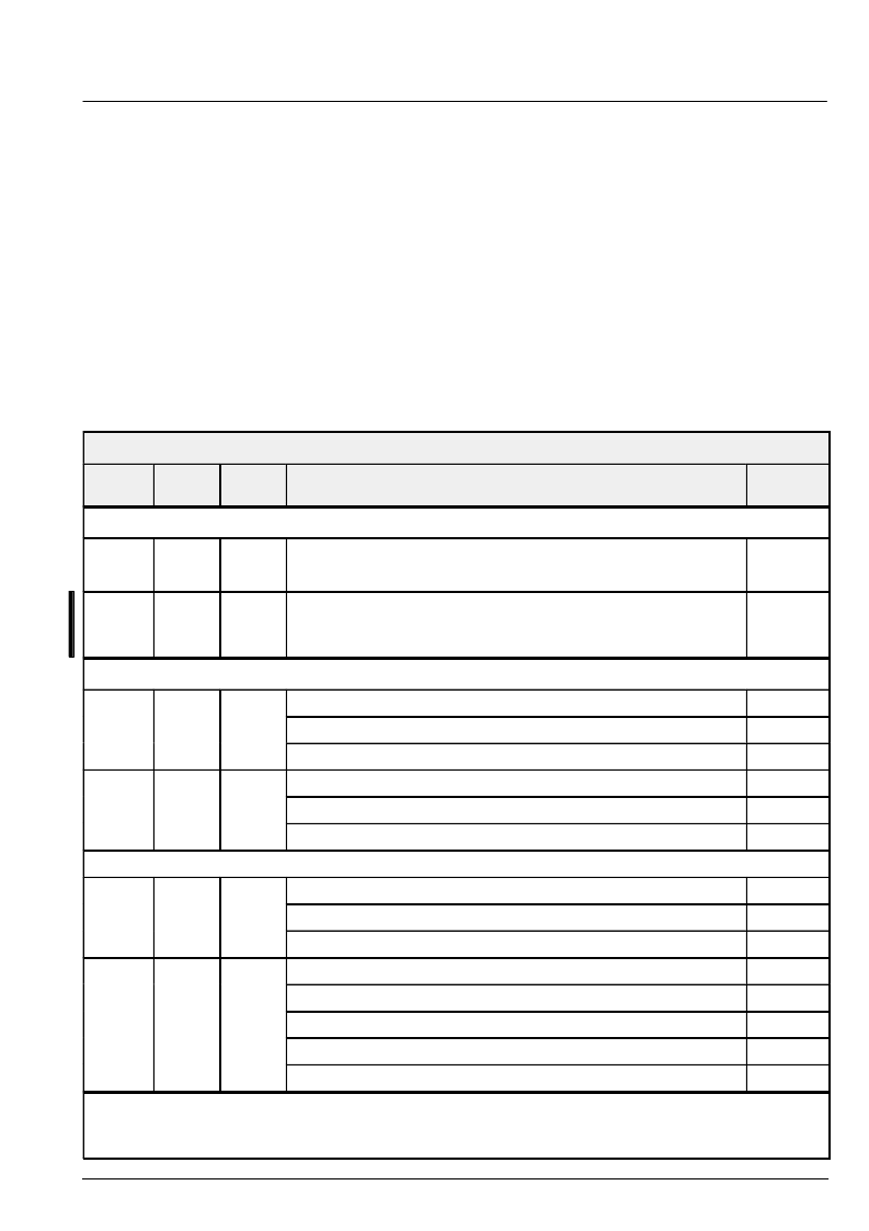
I
2
C-Register Table
I
2
C Reg.
Address
Number
of Bits
Mode
Function
Name
Chip Identification
00
8
r
Manufacture ID in accordance with
JEDEC Solid State Products Engineering Council, Washington DC
INTERMETALL Code EC
hex
I2C_ID0
01 / 02
8 / 8
r
16-bit Part number (01: LSBs, 02: MSBs)
VPX 3220 A
4680
hex
VPX 3216 B
4260
hex
VPX 3214 C
4280
hex
I2C_ID1,
I2C_ID2
Fast Processor (FP)
26
12 / 16
wd
FP read address
FPRD
bit [7:0] :
address
addr
bit [15:8] :
reserved (must be set to zero)
27
12 / 16
wd
FP write address
FPWR
bit [7:0] :
address
addr
bit [15:8] :
reserved (must be set to zero)
Registers 26
hex
and 27
hex
use the same hardware by subaddressing.
28
12 / 16
w
FP data
FPDAT
bit [11:0] :
data
data
bit [15:12] :
reserved (must be set to zero)
29
3 / 8
r
FP status
FPSTA
bit [0] :
write request
bit [1] :
read request
bit [2] :
busy
bit [7:3] :
reserved (return ones)
The control register modes are
– w: write/read register
– d: register is double latched
– A: register is available only in VPX 3220 A; VPX 3216 B returns valid ACK, although no internal action is performed
– r:
– v: register is latched with vsync
read-only register
The mnemonics used in the Intermetall VPX demo software are given in the last column.
相關(guān)PDF資料 |
PDF描述 |
|---|---|
| VPX3214C | Video Pixel Decoders |
| VPX3224D | Video Pixel Decoders |
| VPX3224E | Video Pixel Decoders |
| VPX322XE | Video Pixel Decoders |
| VQ1000J | N-Channel Enhancement-Mode MOSFET Transistor(最小漏源擊穿電壓60V,夾斷電流0.225A的N溝道增強型MOSFET晶體管) |
相關(guān)代理商/技術(shù)參數(shù) |
參數(shù)描述 |
|---|---|
| VPX3214C | 制造商:未知廠家 制造商全稱:未知廠家 功能描述:Video Pixel Decoders |
| VPX3214C(PLCC44) | 制造商:未知廠家 制造商全稱:未知廠家 功能描述:Color Decoder Circuit |
| VPX3214C(QFP44) | 制造商:未知廠家 制造商全稱:未知廠家 功能描述:Color Decoder Circuit |
| VPX3216B | 制造商:未知廠家 制造商全稱:未知廠家 功能描述:Video Pixel Decoders |
| VPX3216B(PLCC44) | 制造商:未知廠家 制造商全稱:未知廠家 功能描述:Color Decoder Circuit |
發(fā)布緊急采購,3分鐘左右您將得到回復(fù)。