- 您現(xiàn)在的位置:買賣IC網(wǎng) > PDF目錄378217 > 82845MZ (INTEL CORP) Intel 845 Family Chipset-Mobile 82845MP/82845MZ Chipset Memory Controller Hub Mobile (MCH-M) PDF資料下載
參數(shù)資料
| 型號: | 82845MZ |
| 廠商: | INTEL CORP |
| 元件分類: | 外設(shè)及接口 |
| 英文描述: | Intel 845 Family Chipset-Mobile 82845MP/82845MZ Chipset Memory Controller Hub Mobile (MCH-M) |
| 中文描述: | MULTIFUNCTION PERIPHERAL, PBGA593 |
| 封裝: | 37.50 X 37.50 MM, FCBGA-593 |
| 文件頁數(shù): | 23/157頁 |
| 文件大?。?/td> | 1407K |
| 代理商: | 82845MZ |
第1頁第2頁第3頁第4頁第5頁第6頁第7頁第8頁第9頁第10頁第11頁第12頁第13頁第14頁第15頁第16頁第17頁第18頁第19頁第20頁第21頁第22頁當前第23頁第24頁第25頁第26頁第27頁第28頁第29頁第30頁第31頁第32頁第33頁第34頁第35頁第36頁第37頁第38頁第39頁第40頁第41頁第42頁第43頁第44頁第45頁第46頁第47頁第48頁第49頁第50頁第51頁第52頁第53頁第54頁第55頁第56頁第57頁第58頁第59頁第60頁第61頁第62頁第63頁第64頁第65頁第66頁第67頁第68頁第69頁第70頁第71頁第72頁第73頁第74頁第75頁第76頁第77頁第78頁第79頁第80頁第81頁第82頁第83頁第84頁第85頁第86頁第87頁第88頁第89頁第90頁第91頁第92頁第93頁第94頁第95頁第96頁第97頁第98頁第99頁第100頁第101頁第102頁第103頁第104頁第105頁第106頁第107頁第108頁第109頁第110頁第111頁第112頁第113頁第114頁第115頁第116頁第117頁第118頁第119頁第120頁第121頁第122頁第123頁第124頁第125頁第126頁第127頁第128頁第129頁第130頁第131頁第132頁第133頁第134頁第135頁第136頁第137頁第138頁第139頁第140頁第141頁第142頁第143頁第144頁第145頁第146頁第147頁第148頁第149頁第150頁第151頁第152頁第153頁第154頁第155頁第156頁第157頁
Intel
82845MP/82845MZ Chipset-Mobile (MCH-M)
250687-002
Datasheet
23
R
2.2.
DDR Interface
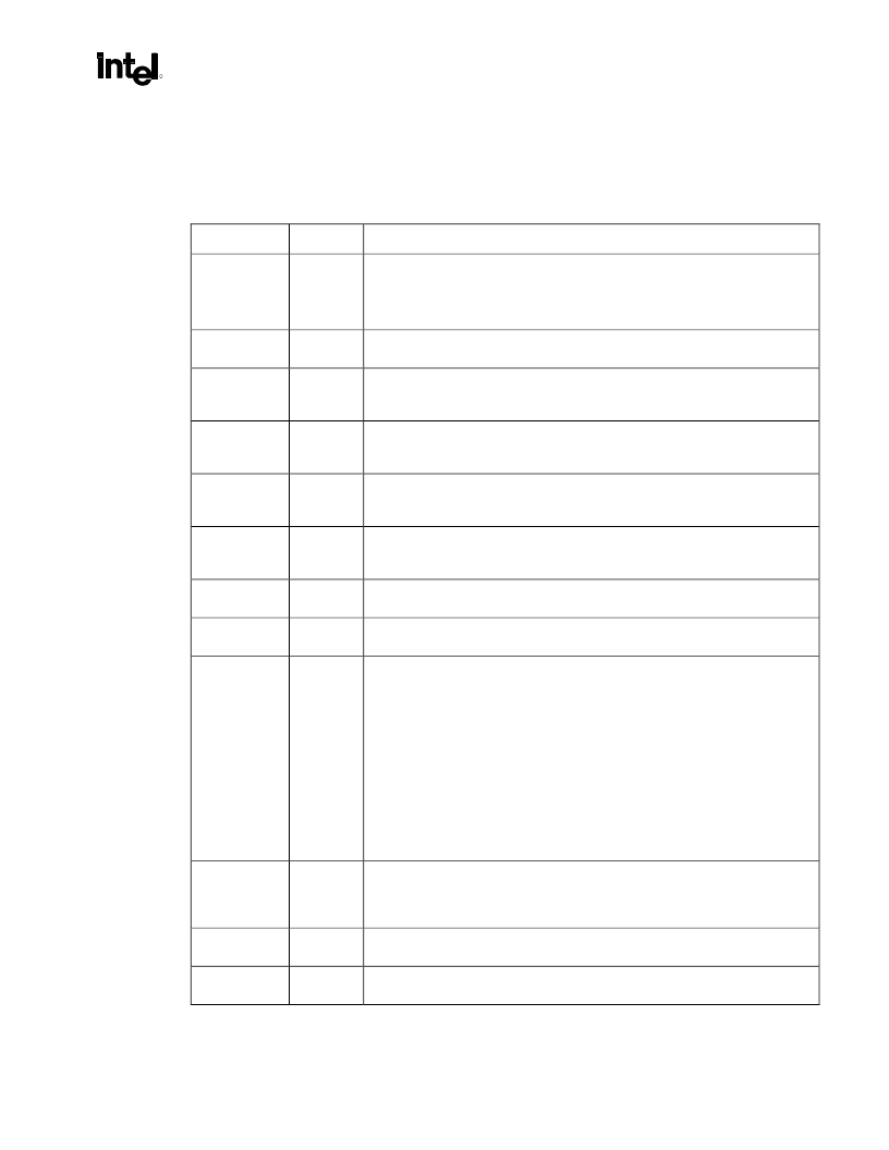
Table 5. DDR Interface Signal Descriptions
Signal Name
Type
Description
SCS#[3:0]
O
CMOS
Chip Select:
These pins select the particular DDR components during the active
state.
Note:
There is one SCS# per DDR-SDRAM Physical SO-DIMM device row. These
signals can be toggled on every rising System Memory Clock edge.
SMA[12:0]
O
CMOS
Multiplexed Memory Address:
These signals are used to provide the multiplexed
row and column address to DDR.
SBS[1:0]
O
CMOS
Memory Bank Address:
These signals define the banks that are selected within
each DDR row. The SMA and SBS signals combine to address every possible
location within a DDR device.
SRAS#
O
CMOS
DDR Row Address Strobe:
SRAS# may be heavily loaded and requires 2 DDR
clock cycles for setup time to the DDRs:
Used with SCAS# and SWE# (along with
SCS#) to define the DRAM commands.
SCAS#
O
CMOS
DDR Column Address Strobe:
SCAS# may be heavily loaded and requires 2 DDR
clock cycles for setup time to the DDRs. Used with SRAS# and SWE# (along with
SCS#) to define the DRAM commands.
SWE#
I/O
CMOS
Write Enable:
Used with SCAS# and SRAS# (along with SCS#) to define the
DRAM commands. SWE# is asserted during writes to DDR. SWE# may be heavily
loaded and requires 2 DDR clock cycles for setup time to the DDRs.
SDQ[63:0]
I/O
CMOS 2X
Data Lines:
These signals are used to interface to the DDR data bus.
SCB[7:0]
I/O
CMOS 2X
Data Lines:
These signals are used to interface to the SDRAM ECC signals (to be
used if SO-DIMMs support ECC).
SDQS[8:0]
I/O
CMOS
Data Strobes:
There is an associated data strobe (DQS) for each data strobe (DQ) and check
bit (CB) group.
SDQS8
-
> SCB[7:0]
SDQS7 -> SDQ[63:56]
SDQS6 -> SDQ[55:48]
SDQS5 -> SDQ[47:40]
SDQS4 -> SDQ[39:32]
SDQS3 -> SDQ[31:24]
SDQS2 -> SDQ[23:16]
SDQS1 -> SDQ[15:8]
SDQS0 -> SDQ[7:0]
SCKE[3:0]
O
CMOS
Clock Enable:
These pins are used to signal a self-refresh or power down
command to a DDR array when entering system suspend. SCKE is also used to
dynamically power down inactive DDR rows. There is one SCKE per DDR row.
These signals can be toggled on every rising SCLK edge.
RCVENOUT#
O
CMOS
Clock Output:
Used to emulate source-synch clocking for reads. Connects to
RCVENIN#.
RCVENIN#
I
CMOS
Clock Input:
Used to emulate source-synch clocking for reads. Connects to
RCVENOUT#.
相關(guān)PDF資料 |
PDF描述 |
|---|---|
| 82845PE | 82845GE Graphics and Memory Controller Hub (GMCH) and 82845PE Memory Controller Hub (MCH) |
| 82845GE | 82845GE Graphics and Memory Controller Hub (GMCH) and 82845PE Memory Controller Hub (MCH) |
| 8284A | Clock Generator and Driver for 8066, 8088 Processors |
| 8284A-1 | Clock Generator and Driver for 8066, 8088 Processors |
| 8284 | TWO-OUTPUT LNB SUPPLY AND CONTROL-VOLTAGE REGULATOR |
相關(guān)代理商/技術(shù)參數(shù) |
參數(shù)描述 |
|---|---|
| 82845PE | 制造商:INTEL 制造商全稱:Intel Corporation 功能描述:82845GE Graphics and Memory Controller Hub (GMCH) and 82845PE Memory Controller Hub (MCH) |
| 8284611SM | 制造商:Thomas & Betts 功能描述: |
| 828461-2 | 制造商:TE Connectivity 功能描述:19P CPC STECK-GEH - Bulk |
| 828462-1 | 制造商:TE Connectivity 功能描述:19P CPC AUFNAHMEGEH - Bulk |
| 828465-000 | 制造商:TE Connectivity 功能描述:Shrink Boot Adapters 180 制造商:TE Connectivity 功能描述:Shrink Boot Adapters 180° 制造商:TE Connectivity 功能描述:TXR40AC00-2418AI - Bulk |
發(fā)布緊急采購,3分鐘左右您將得到回復。