- 您現(xiàn)在的位置:買賣IC網(wǎng) > PDF目錄378217 > 82865G (Intel Corp.) Intel 865G/865GV Graphics and Memory Controller Hub PDF資料下載
參數(shù)資料
| 型號: | 82865G |
| 廠商: | Intel Corp. |
| 英文描述: | Intel 865G/865GV Graphics and Memory Controller Hub |
| 中文描述: | 英特爾865G/865GV圖形和內(nèi)存控制器中樞 |
| 文件頁數(shù): | 192/249頁 |
| 文件大小: | 3540K |
| 代理商: | 82865G |
第1頁第2頁第3頁第4頁第5頁第6頁第7頁第8頁第9頁第10頁第11頁第12頁第13頁第14頁第15頁第16頁第17頁第18頁第19頁第20頁第21頁第22頁第23頁第24頁第25頁第26頁第27頁第28頁第29頁第30頁第31頁第32頁第33頁第34頁第35頁第36頁第37頁第38頁第39頁第40頁第41頁第42頁第43頁第44頁第45頁第46頁第47頁第48頁第49頁第50頁第51頁第52頁第53頁第54頁第55頁第56頁第57頁第58頁第59頁第60頁第61頁第62頁第63頁第64頁第65頁第66頁第67頁第68頁第69頁第70頁第71頁第72頁第73頁第74頁第75頁第76頁第77頁第78頁第79頁第80頁第81頁第82頁第83頁第84頁第85頁第86頁第87頁第88頁第89頁第90頁第91頁第92頁第93頁第94頁第95頁第96頁第97頁第98頁第99頁第100頁第101頁第102頁第103頁第104頁第105頁第106頁第107頁第108頁第109頁第110頁第111頁第112頁第113頁第114頁第115頁第116頁第117頁第118頁第119頁第120頁第121頁第122頁第123頁第124頁第125頁第126頁第127頁第128頁第129頁第130頁第131頁第132頁第133頁第134頁第135頁第136頁第137頁第138頁第139頁第140頁第141頁第142頁第143頁第144頁第145頁第146頁第147頁第148頁第149頁第150頁第151頁第152頁第153頁第154頁第155頁第156頁第157頁第158頁第159頁第160頁第161頁第162頁第163頁第164頁第165頁第166頁第167頁第168頁第169頁第170頁第171頁第172頁第173頁第174頁第175頁第176頁第177頁第178頁第179頁第180頁第181頁第182頁第183頁第184頁第185頁第186頁第187頁第188頁第189頁第190頁第191頁當(dāng)前第192頁第193頁第194頁第195頁第196頁第197頁第198頁第199頁第200頁第201頁第202頁第203頁第204頁第205頁第206頁第207頁第208頁第209頁第210頁第211頁第212頁第213頁第214頁第215頁第216頁第217頁第218頁第219頁第220頁第221頁第222頁第223頁第224頁第225頁第226頁第227頁第228頁第229頁第230頁第231頁第232頁第233頁第234頁第235頁第236頁第237頁第238頁第239頁第240頁第241頁第242頁第243頁第244頁第245頁第246頁第247頁第248頁第249頁
Intel
82865G/82865GV GMCH Datasheet
193
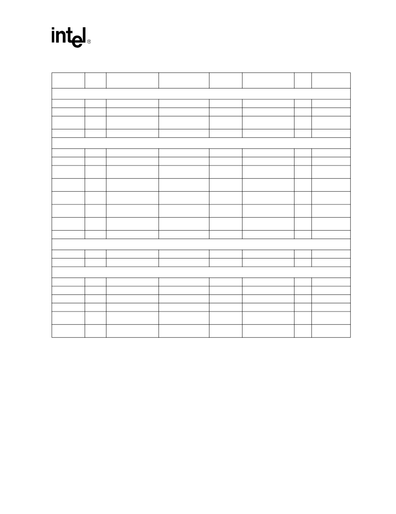
Electrical Characteristics
NOTES:
1. Absolute max overshoot = 4.5 V
2. Crossing voltage is defined as the instantaneous voltage value when the rising edge of HCLKP equals the
falling edge of HCLKN.
3. The crossing point must meet the absolute and relative crossing point specifications simultaneously.
4. V
is the statistical average of the V
measured by the oscilloscope.
5. VHavg can be measured directly using “Vtop” on Agilent* oscilloscopes and “High” on Tektronix
oscilloscopes.
6. Maximum leakage current specification for the GVREF pin is 65 uA. The Maximum leakage current
specification for the GVSWING pin is 50 μA. Refer to
Intel
865G/865GV/865PE/865P Chipset Platform
Design Guide
for the resistor divider circuit details that take this specification into account.
7. Maximum leakage current specification for HI_VREF and HI_SWING pins is 50 μA. Refer to 865G
/865GV
/
865PE/865P Chipset Platform Design Guide for the resistor divider circuit details that take this specification
into account.
8. Maximum leakage current specification for CI_VREF and CI_SWING pins is 50 μA. Refer to 865G
/865GV
/
865PE Chipset Platform Design Guide for the resistor divider circuit details that take this specification into
account.
2.6 V Miscellaneous Signals (3.3 V tolerant)
V
IL
(t)
2.6 V Input Low Voltage
0.4
V
V
IH
(t)
2.6 V Input High Voltage
VCC_DDR – 0.4
VCC_DAC
V
I
LEAK
(t)
2.6 V Input Leakage
Current
±50
μ
A
C
IN
(t)
2.6 V Input Capacitance
5.5
pF
3.3 V Miscellaneous Signals
V
IL
(o)
3.3V Input Low Voltage
0.4
V
V
IH
(o)
3.3 V Input High Voltage
VCC_DAC – 0.4
VCC_DAC
V
V
OL
(o)
3.3 V Output Low
Voltage
0.2
V
V
OH
(o)
3.3 V Output High
Voltage
VCC_DAC – 0.2
V
I
OL
(o)
3.3 V Output Low
Current
50
mA
@V
OL
max
I
OH
(o)
3.3 V Output High
Current
–50
mA
@V
OH
min
I
LEAK
(o)
3.3 V Input Leakage
Current
±50
μ
A
C
IN
(o)
3.3 V Input Capacitance
5.5
pF
FSB Select Signals
V
IL
(w)
Input Low Voltage
0.4
V
V
IH
(w)
Input High Voltage
0.8
V
Clocks
V
IL
(x)
Input Low Voltage
0.4
V
V
IH
(x)
Input High Voltage
VCC_DDR – 0.4
VCC_DAC
V
1
I
LEAK
(x)
Input Leakage Current
100
μ
A
C
IN
(x)
Input Capacitance
5.5
pF
V
CROSS(abs)
(j)
Absolute Crossing
Voltage
0.250
NA
0.550
V
2,3
V
CROSS(rel)
(j)
Relative Crossing
Voltage
0.250 + 0.5
(V
Havg
– 0.700)
0.550 +
0.5(V
Havg
– 0.700)
V
3,4,5
Table 38. DC Characteristics (Sheet 3 of 3)
Symbol
Signal
Group
Parameter
Min
Nom
Max
Unit
Notes
相關(guān)PDF資料 |
PDF描述 |
|---|---|
| 82865GV | Intel 865G/865GV Graphics and Memory Controller Hub |
| 8288 | Bus Controller for SAB 8086 Family Processors |
| 828 | 2 X 2 8-Pole Filters |
| 8291A | GPIB TALKER/LISTENER |
| 829B | SILICON 28V HYPERABRUPT VARACTOR DIODES |
相關(guān)代理商/技術(shù)參數(shù) |
參數(shù)描述 |
|---|---|
| 82865GV | 制造商:INTEL 制造商全稱:Intel Corporation 功能描述:Intel 865G/865GV Graphics and Memory Controller Hub |
| 82865N | 功能描述:HEX DIE 5/8-11 制造商:apex tool group 系列:* 零件狀態(tài):在售 標(biāo)準(zhǔn)包裝:1 |
| 828661-1 | 功能描述:汽車連接器 25P JUN-TIMER CONN RoHS:否 制造商:Amphenol SINE Systems 產(chǎn)品:Contacts 系列:ATP 位置數(shù)量: 型式:Female 安裝風(fēng)格: 端接類型: 觸點(diǎn)電鍍:Nickel |
| 828662-1 | 制造商:TE Connectivity 功能描述:CONN TIMER CONN M 16 POS 5MM SLDR ST TH - Bulk 制造商:TE Connectivity 功能描述:16P JUN-TIMER STECK 制造商:TE Connectivity 功能描述:Conn Timer Connector M 16 POS 5mm Solder ST Thru-Hole |
| 82866N | 功能描述:HEX DIE 5/8-18 制造商:apex tool group 系列:* 零件狀態(tài):在售 標(biāo)準(zhǔn)包裝:1 |
發(fā)布緊急采購,3分鐘左右您將得到回復(fù)。