- 您現(xiàn)在的位置:買賣IC網(wǎng) > PDF目錄378217 > 82865GV (Intel Corp.) Intel 865G/865GV Graphics and Memory Controller Hub PDF資料下載
參數(shù)資料
| 型號: | 82865GV |
| 廠商: | Intel Corp. |
| 英文描述: | Intel 865G/865GV Graphics and Memory Controller Hub |
| 中文描述: | 英特爾865G/865GV圖形和內(nèi)存控制器中樞 |
| 文件頁數(shù): | 98/249頁 |
| 文件大小: | 3540K |
| 代理商: | 82865GV |
第1頁第2頁第3頁第4頁第5頁第6頁第7頁第8頁第9頁第10頁第11頁第12頁第13頁第14頁第15頁第16頁第17頁第18頁第19頁第20頁第21頁第22頁第23頁第24頁第25頁第26頁第27頁第28頁第29頁第30頁第31頁第32頁第33頁第34頁第35頁第36頁第37頁第38頁第39頁第40頁第41頁第42頁第43頁第44頁第45頁第46頁第47頁第48頁第49頁第50頁第51頁第52頁第53頁第54頁第55頁第56頁第57頁第58頁第59頁第60頁第61頁第62頁第63頁第64頁第65頁第66頁第67頁第68頁第69頁第70頁第71頁第72頁第73頁第74頁第75頁第76頁第77頁第78頁第79頁第80頁第81頁第82頁第83頁第84頁第85頁第86頁第87頁第88頁第89頁第90頁第91頁第92頁第93頁第94頁第95頁第96頁第97頁當(dāng)前第98頁第99頁第100頁第101頁第102頁第103頁第104頁第105頁第106頁第107頁第108頁第109頁第110頁第111頁第112頁第113頁第114頁第115頁第116頁第117頁第118頁第119頁第120頁第121頁第122頁第123頁第124頁第125頁第126頁第127頁第128頁第129頁第130頁第131頁第132頁第133頁第134頁第135頁第136頁第137頁第138頁第139頁第140頁第141頁第142頁第143頁第144頁第145頁第146頁第147頁第148頁第149頁第150頁第151頁第152頁第153頁第154頁第155頁第156頁第157頁第158頁第159頁第160頁第161頁第162頁第163頁第164頁第165頁第166頁第167頁第168頁第169頁第170頁第171頁第172頁第173頁第174頁第175頁第176頁第177頁第178頁第179頁第180頁第181頁第182頁第183頁第184頁第185頁第186頁第187頁第188頁第189頁第190頁第191頁第192頁第193頁第194頁第195頁第196頁第197頁第198頁第199頁第200頁第201頁第202頁第203頁第204頁第205頁第206頁第207頁第208頁第209頁第210頁第211頁第212頁第213頁第214頁第215頁第216頁第217頁第218頁第219頁第220頁第221頁第222頁第223頁第224頁第225頁第226頁第227頁第228頁第229頁第230頁第231頁第232頁第233頁第234頁第235頁第236頁第237頁第238頁第239頁第240頁第241頁第242頁第243頁第244頁第245頁第246頁第247頁第248頁第249頁
Intel
82865G/82865GV GMCH Datasheet
99
Register Description
3.6.21
BCTRL1—Bridge Control Register (Device 1)
Address Offset:
Default Value:
Access:
Size:
3Eh
00h
RO, R/W
8 bits
This register provides extensions to the PCICMD1 register that are specific to PCI-to-PCI bridges.
The BCTRL1 provides additional control for the secondary interface (i.e., PCI_B/AGP) as well as
some bits that affect the overall behavior of the virtual PCI-to-PCI bridge in the GMCH
(e.g., VGA compatible address ranges mapping).
The bit field definitions for VGAEN and MDAP are detailed in
Table 9
.
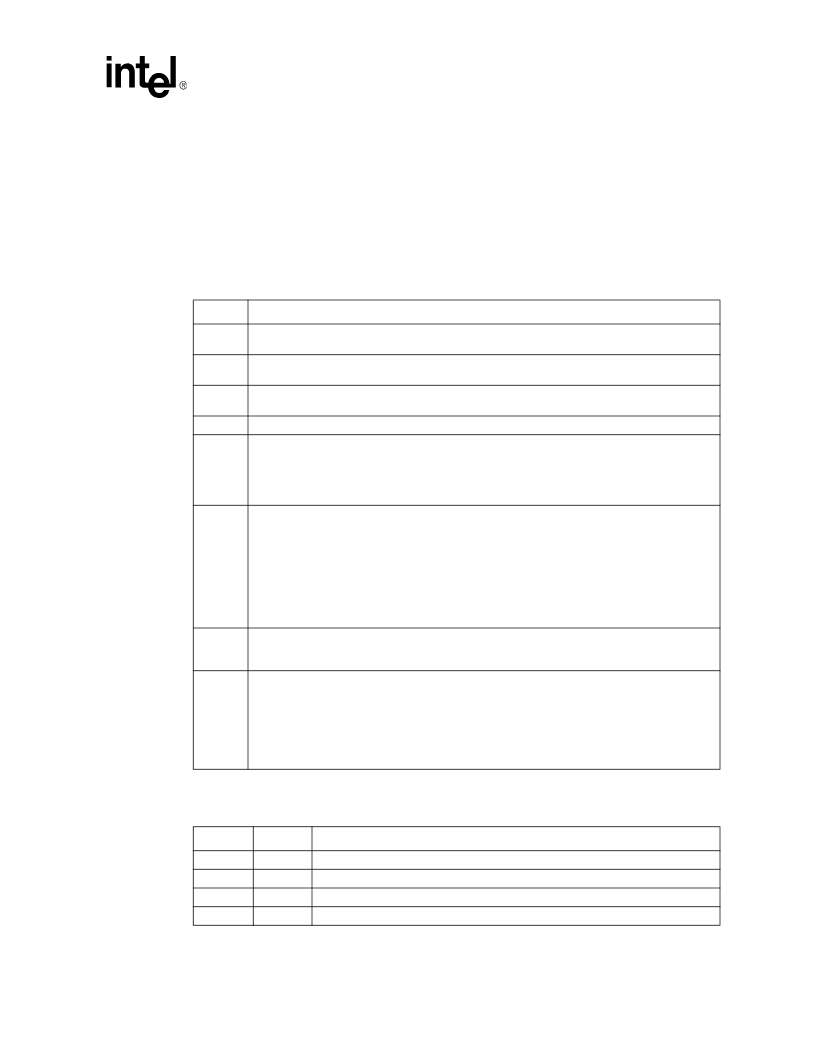
Bit
Descriptions
7
Fast Back-to-Back Enable (FB2BEN)—RO.
Hardwired to 0. GMCH does not generate fast back-
to-back cycles as a master on AGP.
6
Secondary Bus Reset (SRESET)—RO.
Hardwired to 0. GMCH does not support generation of
reset via this bit on the AGP.
5
Master Abort Mode (MAMODE)—RO.
Hardwired to 0. Thus, when acting as a master on AGP/
PCI_B, the GMCH will discard writes and return all 1s during reads when a master abort occurs.
4
Reserved.
3
VGA Enable (VGAEN)—R/W.
This bit controls the routing of processor-initiated transactions
targeting VGA compatible I/O and memory address ranges. This bit works in conjunction with the
GMCHCFG[MDAP] bit (offset C6h) as described in
Table 9
.
0 = Disable
1 = Enable
2
ISA Enable (ISAEN)—R/W.
This bit modifies the response by the GMCH to an I/O access issued
by the processor that target ISA I/O addresses. This applies only to I/O addresses that are enabled
by the IOBASE and IOLIMIT registers.
0 =All addresses defined by the IOBASE and IOLIMIT for processor I/O transactions are mapped
to PCI_B/AGP. (default)
1 =The GMCH does not forward to PCI_B/AGP any I/O transactions addressing the last 768 bytes
in each 1-KB block, even if the addresses are within the range defined by the IOBASE and
IOLIMIT registers. Instead of going to PCI_B/AGP these cycles are forwarded to HI where
they can be subtractively or positively claimed by the ISA bridge.
1
SERR Enable (SERREN)—RO.
Hardwired to 0. This bit normally controls forwarding SERR# on
the secondary interface to the primary interface. The GMCH does not support the SERR# signal
on the AGP/PCI_B bus.
0
Parity Error Response Enable (PEREN)—R/W.
This bit controls the GMCH’s response to data
phase parity errors on PCI_B/AGP. G_PERR# is not implemented by the GMCH.
0 =Disable. Address and data parity errors on PCI_B/AGP are not reported via the GMCH HI
SERR messaging mechanism. Other types of error conditions can still be signaled via SERR
messaging independent of this bit’s state.
1 =Enable. Address and data parity errors detected on PCI_B are reported via the HI SERR
messaging mechanism, if further enabled by SERRE1.
Table 9. VGAEN and MDAP Field Definitions
VGAEN
MDAP
Description
0
0
All References to MDA and VGA space are routed to HI.
0
1
Illegal combination.
1
0
All VGA references are routed to this bus. MDA references are routed to HI.
1
1
All VGA references are routed to this bus. MDA references are routed to HI.
相關(guān)PDF資料 |
PDF描述 |
|---|---|
| 8288 | Bus Controller for SAB 8086 Family Processors |
| 828 | 2 X 2 8-Pole Filters |
| 8291A | GPIB TALKER/LISTENER |
| 829B | SILICON 28V HYPERABRUPT VARACTOR DIODES |
| 829A | SILICON 28V HYPERABRUPT VARACTOR DIODES |
相關(guān)代理商/技術(shù)參數(shù) |
參數(shù)描述 |
|---|---|
| 82865N | 功能描述:HEX DIE 5/8-11 制造商:apex tool group 系列:* 零件狀態(tài):在售 標(biāo)準(zhǔn)包裝:1 |
| 828661-1 | 功能描述:汽車連接器 25P JUN-TIMER CONN RoHS:否 制造商:Amphenol SINE Systems 產(chǎn)品:Contacts 系列:ATP 位置數(shù)量: 型式:Female 安裝風(fēng)格: 端接類型: 觸點(diǎn)電鍍:Nickel |
| 828662-1 | 制造商:TE Connectivity 功能描述:CONN TIMER CONN M 16 POS 5MM SLDR ST TH - Bulk 制造商:TE Connectivity 功能描述:16P JUN-TIMER STECK 制造商:TE Connectivity 功能描述:Conn Timer Connector M 16 POS 5mm Solder ST Thru-Hole |
| 82866N | 功能描述:HEX DIE 5/8-18 制造商:apex tool group 系列:* 零件狀態(tài):在售 標(biāo)準(zhǔn)包裝:1 |
| 82867001 | 制造商:未知廠家 制造商全稱:未知廠家 功能描述:MOTOR GEARED 12VDC 344RPM |
發(fā)布緊急采購,3分鐘左右您將得到回復(fù)。