- 您現(xiàn)在的位置:買賣IC網(wǎng) > PDF目錄298975 > CY7C1339G-200AXCT (CYPRESS SEMICONDUCTOR CORP) 128K X 32 CACHE SRAM, 2.8 ns, PQFP100 PDF資料下載
參數(shù)資料
| 型號(hào): | CY7C1339G-200AXCT |
| 廠商: | CYPRESS SEMICONDUCTOR CORP |
| 元件分類: | SRAM |
| 英文描述: | 128K X 32 CACHE SRAM, 2.8 ns, PQFP100 |
| 封裝: | 14 X 20 MM, 1.40 MM HEIGHT, LEAD FREE, MS-026, TQFP-100 |
| 文件頁(yè)數(shù): | 13/18頁(yè) |
| 文件大?。?/td> | 386K |
| 代理商: | CY7C1339G-200AXCT |
第1頁(yè)第2頁(yè)第3頁(yè)第4頁(yè)第5頁(yè)第6頁(yè)第7頁(yè)第8頁(yè)第9頁(yè)第10頁(yè)第11頁(yè)第12頁(yè)當(dāng)前第13頁(yè)第14頁(yè)第15頁(yè)第16頁(yè)第17頁(yè)第18頁(yè)
CY7C1339G
Document #: 38-05520 Rev. *F
Page 4 of 18
Functional Overview
All synchronous inputs pass through input registers controlled
by the rising edge of the clock. All data outputs pass through
output registers controlled by the rising edge of the clock.
Maximum access delay from the clock rise (tCO) is 2.6 ns
(250-MHz device).
The CY7C1339G supports secondary cache in systems
utilizing either a linear or interleaved burst sequence. The
interleaved
burst
order
supports
Pentium
and
i486
processors. The linear burst sequence is suited for processors
that utilize a linear burst sequence. The burst order is user
selectable, and is determined by sampling the MODE input.
Accesses can be initiated with either the Processor Address
Strobe (ADSP) or the Controller Address Strobe (ADSC).
Address advancement through the burst sequence is
controlled by the ADV input. A two-bit on-chip wraparound
burst counter captures the first address in a burst sequence
and automatically increments the address for the rest of the
burst access.
Byte Write operations are qualified with the Byte Write Enable
(BWE) and Byte Write Select (BW[A:D]) inputs. A Global Write
Enable (GW) overrides all Byte Write inputs and writes data to
all four bytes. All writes are simplified with on-chip
synchronous self-timed Write circuitry.
Three synchronous Chip Selects (CE1, CE2, CE3) and an
asynchronous Output Enable (OE) provide for easy bank
selection and output tri-state control. ADSP is ignored if CE1
is HIGH.
Single Read Accesses
This access is initiated when the following conditions are
satisfied at clock rise: (1) ADSP or ADSC is asserted LOW, (2)
CE1, CE2, CE3 are all asserted active, and (3) the Write
signals (GW, BWE) are all deserted HIGH. ADSP is ignored if
CE1 is HIGH. The address presented to the address inputs (A)
is stored into the address advancement logic and the Address
Register while being presented to the memory array. The
corresponding data is allowed to propagate to the input of the
Output Registers. At the rising edge of the next clock the data
is allowed to propagate through the output register and onto
the data bus within 2.6 ns (250-MHz device) if OE is active
LOW. The only exception occurs when the SRAM is emerging
from a deselected state to a selected state, its outputs are
always tri-stated during the first cycle of the access. After the
first cycle of the access, the outputs are controlled by the OE
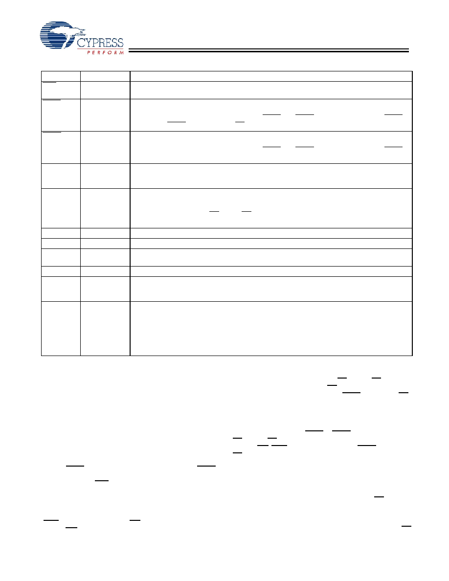
ADV
Input-
Synchronous
Advance Input signal, sampled on the rising edge of CLK, active LOW. When asserted, it
automatically increments the address in a burst cycle.
ADSP
Input-
Synchronous
Address Strobe from Processor, sampled on the rising edge of CLK, active LOW. When
asserted LOW, addresses presented to the device are captured in the address registers. A1, A0
are also loaded into the burst counter. When ADSP and ADSC are both asserted, only ADSP is
recognized. ASDP is ignored when CE1 is deasserted HIGH.
ADSC
Input-
Synchronous
Address Strobe from Controller, sampled on the rising edge of CLK, active LOW. When
asserted LOW, addresses presented to the device are captured in the address registers. A1, A0
are also loaded into the burst counter. When ADSP and ADSC are both asserted, only ADSP is
recognized.
ZZ
Input-
Asynchronous
ZZ “sleep” Input, active HIGH. When asserted HIGH places the device in a non-time-critical
“sleep” condition with data integrity preserved. For normal operation, this pin has to be LOW or
left floating. ZZ pin has an internal pull-down.
DQs
I/O-
Synchronous
Bidirectional Data I/O lines. As inputs, they feed into an on-chip data register that is triggered
by the rising edge of CLK. As outputs, they deliver the data contained in the memory location
specified by the addresses presented during the previous clock rise of the read cycle. The direction
of the pins is controlled by OE. When OE is asserted LOW, the pins behave as outputs. When
HIGH, DQs are placed in a tri-state condition.
VDD
Power Supply Power supply inputs to the core of the device.
VSS
Ground
Ground for the core of the device.
VDDQ
I/O Power
Supply
Power supply for the I/O circuitry.
VSSQ
I/O Ground
Ground for the I/O circuitry.
MODE
Input-
Static
Selects Burst Order. When tied to GND selects linear burst sequence. When tied to VDD or left
floating selects interleaved burst sequence. This is a strap pin and should remain static during
device operation. Mode Pin has an internal pull-up.
NC,NC/9M,
NC/18M.
NC/72M,
NC/144M,
NC/288M,
NC/576M,
NC/1G
–
No Connects. Not internally connected to the die. NC/9M, NC/18M, NC/72M, NC/144M,
NC/288M, NC/576M and NC/1G are address expansion pins are not internally connected to the
die.
Pin Definitions (continued)
Name
I/O
Description
相關(guān)PDF資料 |
PDF描述 |
|---|---|
| CY7C1347D-250BGC | 128K X 36 CACHE SRAM, 2.4 ns, PBGA119 |
| CY7C1512JV18-267BZXC | 4M X 18 QDR SRAM, 0.45 ns, PBGA165 |
| CY7C1515AV18-250BZXI | 2M X 36 QDR SRAM, 0.45 ns, PBGA165 |
| CY7C1522JV18-250BZI | 8M X 8 DDR SRAM, 0.45 ns, PBGA165 |
| CY7C1524KV18-333BZI | 2M X 36 DDR SRAM, 0.45 ns, PBGA165 |
相關(guān)代理商/技術(shù)參數(shù) |
參數(shù)描述 |
|---|---|
| CY7C1339G-200BGI | 功能描述:靜態(tài)隨機(jī)存取存儲(chǔ)器 128Kx32 3.3V IND Sync FT 靜態(tài)隨機(jī)存取存儲(chǔ)器 RoHS:否 制造商:Cypress Semiconductor 存儲(chǔ)容量:16 Mbit 組織:1 M x 16 訪問(wèn)時(shí)間:55 ns 電源電壓-最大:3.6 V 電源電壓-最小:2.2 V 最大工作電流:22 uA 最大工作溫度:+ 85 C 最小工作溫度:- 40 C 安裝風(fēng)格:SMD/SMT 封裝 / 箱體:TSOP-48 封裝:Tray |
| CY7C1339G-200BGIT | 功能描述:靜態(tài)隨機(jī)存取存儲(chǔ)器 128Kx32 3.3V IND Sync FT 靜態(tài)隨機(jī)存取存儲(chǔ)器 RoHS:否 制造商:Cypress Semiconductor 存儲(chǔ)容量:16 Mbit 組織:1 M x 16 訪問(wèn)時(shí)間:55 ns 電源電壓-最大:3.6 V 電源電壓-最小:2.2 V 最大工作電流:22 uA 最大工作溫度:+ 85 C 最小工作溫度:- 40 C 安裝風(fēng)格:SMD/SMT 封裝 / 箱體:TSOP-48 封裝:Tray |
| CY7C1339G-200BGXI | 制造商:Cypress Semiconductor 功能描述:SRAM SYNC QUAD 3.3V 4MBIT 128KX32 2.8NS 119BGA - Bulk |
| CY7C1339L-15ZIT | 制造商:Cypress Semiconductor 功能描述:ELECTRONIC COMPONENT |
| CY7C1339S-133AXC | 功能描述:靜態(tài)隨機(jī)存取存儲(chǔ)器 CY7C1339S-133AXC RoHS:否 制造商:Cypress Semiconductor 存儲(chǔ)容量:16 Mbit 組織:1 M x 16 訪問(wèn)時(shí)間:55 ns 電源電壓-最大:3.6 V 電源電壓-最小:2.2 V 最大工作電流:22 uA 最大工作溫度:+ 85 C 最小工作溫度:- 40 C 安裝風(fēng)格:SMD/SMT 封裝 / 箱體:TSOP-48 封裝:Tray |
發(fā)布緊急采購(gòu),3分鐘左右您將得到回復(fù)。