- 您現(xiàn)在的位置:買賣IC網(wǎng) > PDF目錄298975 > CY7C1524KV18-333BZI (CYPRESS SEMICONDUCTOR CORP) 2M X 36 DDR SRAM, 0.45 ns, PBGA165 PDF資料下載
參數(shù)資料
| 型號: | CY7C1524KV18-333BZI |
| 廠商: | CYPRESS SEMICONDUCTOR CORP |
| 元件分類: | SRAM |
| 英文描述: | 2M X 36 DDR SRAM, 0.45 ns, PBGA165 |
| 封裝: | 15 X 13 MM, 1.40 MM HEIGHT, MO-216, FBGA-165 |
| 文件頁數(shù): | 3/32頁 |
| 文件大小: | 883K |
| 代理商: | CY7C1524KV18-333BZI |
第1頁第2頁當前第3頁第4頁第5頁第6頁第7頁第8頁第9頁第10頁第11頁第12頁第13頁第14頁第15頁第16頁第17頁第18頁第19頁第20頁第21頁第22頁第23頁第24頁第25頁第26頁第27頁第28頁第29頁第30頁第31頁第32頁
CY7C1522KV18, CY7C1529KV18
CY7C1523KV18, CY7C1524KV18
Document Number: 001-00438 Rev. *F
Page 11 of 32
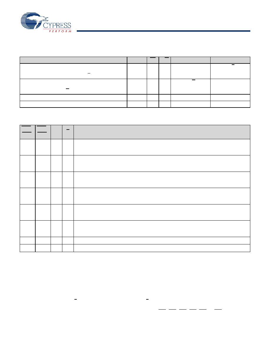
Truth Table
The truth table for CY7C1522KV18, CY7C1529KV18, CY7C1523KV18, and CY7C1524KV18 follows. [2, 3, 4, 5, 6, 7]
Operation
K
LD
R/W
DQ
Write Cycle:
Load address; wait one cycle;
input write data on consecutive K and K rising edges.
L-H
L
D(A + 0) at K(t + 1)
↑ D(A + 1) at K(t + 1)↑
Read Cycle:
Load address; wait one and a half cycle;
read data on consecutive C and C rising edges.
L-H
L
H
Q(A + 0) at C(t + 1)
↑ Q(A + 1) at C(t + 2)↑
NOP: No Operation
L-H
H
X
High-Z
Standby: Clock Stopped
Stopped
X
Previous State
Write Cycle Descriptions
The write cycle description table for CY7C1522KV18 and CY7C1523KV18 follows. [2, 8]
BWS0/
NWS0
BWS1/
NWS1
K
Comments
L
L–H
–
During the data portion of a write sequence
:
CY7C1522KV18
both nibbles (D[7:0]) are written into the device.
CY7C1523KV18
both bytes (D[17:0]) are written into the device.
L
–
L-H During the data portion of a write sequence
:
CY7C1522KV18
both nibbles (D[7:0]) are written into the device.
CY7C1523KV18
both bytes (D[17:0]) are written into the device.
L
H
L–H
–
During the data portion of a write sequence
:
CY7C1522KV18
only the lower nibble (D[3:0]) is written into the device, D[7:4] remains unaltered.
CY7C1523KV18
only the lower byte (D[8:0]) is written into the device, D[17:9] remains unaltered.
L
H
–
L–H During the data portion of a write sequence
:
CY7C1522KV18
only the lower nibble (D[3:0]) is written into the device, D[7:4] remains unaltered.
CY7C1523KV18
only the lower byte (D[8:0]) is written into the device, D[17:9] remains unaltered.
H
L
L–H
–
During the data portion of a write sequence
:
CY7C1522KV18
only the upper nibble (D[7:4]) is written into the device, D[3:0] remains unaltered.
CY7C1523KV18
only the upper byte (D[17:9]) is written into the device, D[8:0] remains unaltered.
H
L
–
L–H During the data portion of a write sequence
:
CY7C1522KV18
only the upper nibble (D[7:4]) is written into the device, D[3:0] remains unaltered.
CY7C1523KV18
only the upper byte (D[17:9]) is written into the device, D[8:0] remains unaltered.
H
L–H
–
No data is written into the devices during this portion of a write operation.
H
–
L–H No data is written into the devices during this portion of a write operation.
Notes
2. X = “Don't Care,” H = Logic HIGH, L = Logic LOW,
↑represents rising edge.
3. Device powers up deselected with the outputs in a tristate condition.
4. “A” represents address location latched by the devices when transaction was initiated. A + 0, A + 1 represents the internal address sequence in the burst.
5. “t” represents the cycle at which a read/write operation is started. t + 1, and t + 2 are the first, and second clock cycles respectively succeeding the “t” clock cycle.
6. Data inputs are registered at K and K rising edges. Data outputs are delivered on C and C rising edges, except when in single clock mode.
7. Ensure that when the clock is stopped K = K and C = C = HIGH. This is not essential, but permits most rapid restart by overcoming transmission line charging
symmetrically.
8. Is based on a write cycle that was initiated in accordance with the Write Cycle Descriptions table. NWS0, NWS1, BWS0, BWS1, BWS2,and BWS3 can be altered on
different portions of a write cycle, as long as the setup and hold requirements are achieved.
相關PDF資料 |
PDF描述 |
|---|---|
| CY7C1612KV18-333BZXC | 8M X 18 QDR SRAM, PBGA165 |
| CY7C256-45PC | 32K X 8 OTPROM, 45 ns, PDIP28 |
| CY7C2561KV18-450BZC | 8M X 8 QDR SRAM, 0.37 ns, PBGA165 |
| CY7C2566KV18-450BZI | 8M X 8 DDR SRAM, 0.37 ns, PBGA165 |
| CY7C293AL-35WC | 2K X 8 UVPROM, 35 ns, CDIP24 |
相關代理商/技術參數(shù) |
參數(shù)描述 |
|---|---|
| CY7C1525JV18250BZC | 制造商:Cypress Semiconductor 功能描述: |
| CY7C1525JV18-250BZC | 功能描述:靜態(tài)隨機存取存儲器 8M x 9 1.8V QDR-II 靜態(tài)隨機存取存儲器 Two-Word Burst RoHS:否 制造商:Cypress Semiconductor 存儲容量:16 Mbit 組織:1 M x 16 訪問時間:55 ns 電源電壓-最大:3.6 V 電源電壓-最小:2.2 V 最大工作電流:22 uA 最大工作溫度:+ 85 C 最小工作溫度:- 40 C 安裝風格:SMD/SMT 封裝 / 箱體:TSOP-48 封裝:Tray |
| CY7C1525JV18-250BZCES | 制造商:Rochester Electronics LLC 功能描述: 制造商:Cypress Semiconductor 功能描述: |
| CY7C1525JV18-250BZXC | 功能描述:靜態(tài)隨機存取存儲器 8M x 9 1.8V QDR-II 靜態(tài)隨機存取存儲器 Two-Word Burst RoHS:否 制造商:Cypress Semiconductor 存儲容量:16 Mbit 組織:1 M x 16 訪問時間:55 ns 電源電壓-最大:3.6 V 電源電壓-最小:2.2 V 最大工作電流:22 uA 最大工作溫度:+ 85 C 最小工作溫度:- 40 C 安裝風格:SMD/SMT 封裝 / 箱體:TSOP-48 封裝:Tray |
| CY7C1525KV18-250BZC | 功能描述:靜態(tài)隨機存取存儲器 72MB (8Mx9) 1.8v 250MHz QDR II 靜態(tài)隨機存取存儲器 RoHS:否 制造商:Cypress Semiconductor 存儲容量:16 Mbit 組織:1 M x 16 訪問時間:55 ns 電源電壓-最大:3.6 V 電源電壓-最小:2.2 V 最大工作電流:22 uA 最大工作溫度:+ 85 C 最小工作溫度:- 40 C 安裝風格:SMD/SMT 封裝 / 箱體:TSOP-48 封裝:Tray |
發(fā)布緊急采購,3分鐘左右您將得到回復。