- 您現(xiàn)在的位置:買賣IC網(wǎng) > PDF目錄373069 > K4T1G044QQ-HC(L)E6 (SAMSUNG SEMICONDUCTOR CO. LTD.) 1Gb Q-die DDR2 SDRAM Specification PDF資料下載
參數(shù)資料
| 型號: | K4T1G044QQ-HC(L)E6 |
| 廠商: | SAMSUNG SEMICONDUCTOR CO. LTD. |
| 英文描述: | 1Gb Q-die DDR2 SDRAM Specification |
| 中文描述: | 1Gb的調(diào)Q DDR2內(nèi)存芯片規(guī)格 |
| 文件頁數(shù): | 4/44頁 |
| 文件大小: | 891K |
| 代理商: | K4T1G044QQ-HC(L)E6 |
第1頁第2頁第3頁當(dāng)前第4頁第5頁第6頁第7頁第8頁第9頁第10頁第11頁第12頁第13頁第14頁第15頁第16頁第17頁第18頁第19頁第20頁第21頁第22頁第23頁第24頁第25頁第26頁第27頁第28頁第29頁第30頁第31頁第32頁第33頁第34頁第35頁第36頁第37頁第38頁第39頁第40頁第41頁第42頁第43頁第44頁
K4T1G084QQ
K4T1G164QQ
Rev. 1.01 November 2007
DDR2 SDRAM
4 of 44
K4T1G044QQ
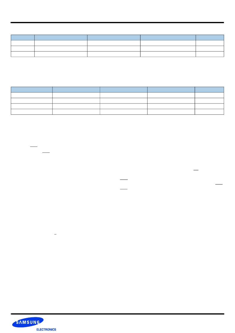
Speed
DDR2-800 5-5-5
DDR2-800 6-6-6
DDR2-667 5-5-5
Units
CAS Latency
5
6
5
tCK
tRCD(min)
12.5
15
15
ns
tRP(min)
12.5
15
15
ns
tRC(min)
57.5
60
60
ns
Note :
1. Speed bin is in order of CL-tRCD-tRP.
2. RoHS Compliant.
3. “H” of Part number(12th digit) stand for RoHS compliant and Halogen-free products.
Org.
DDR2-800 5-5-5
DDR2-800 6-6-6
DDR2-667 5-5-5
Package
256Mx4
K4T1G044QQ-HC(L)E7
K4T1G044QQ-HC(L)F7
K4T1G044QQ-HC(L)E6
60 FBGA
128Mx8
K4T1G084QQ-HC(L)E7
K4T1G084QQ-HC(L)F7
K4T1G084QQ-HC(L)E6
60 FBGA
64Mx16
K4T1G164QQ-HC(L)E7
K4T1G164QQ-HC(L)F7
K4T1G164QQ-HC(L)E6
84 FBGA
JEDEC standard 1.8V ± 0.1V Power Supply
VDDQ = 1.8V ± 0.1V
333MHz f
CK
for 667Mb/sec/pin, 400MHz f
CK
for 800Mb/sec/
pin
8 Banks
Posted CAS
Programmable CAS Latency: 3, 4, 5, 6
Programmable Additive Latency: 0, 1, 2, 3, 4, 5
Write Latency(WL) = Read Latency(RL) -1
Burst Length: 4 , 8(Interleave/nibble sequential)
Programmable Sequential / Interleave Burst Mode
Bi-directional Differential Data-Strobe (Single-ended data-
strobe is an optional feature)
Off-Chip Driver(OCD) Impedance Adjustment
On Die Termination
Special Function Support
- PASR(Partial Array Self Refresh)
- 50ohm ODT
- High Temperature Self-Refresh rate enable
Average Refresh Period 7.8us at lower than T
CASE
85
°
C,
3.9us at 85
°
C < T
CASE
< 95
°
C
All of Lead-free products are compliant for RoHS
The 1Gb DDR2 SDRAM is organized as a 32Mbit x 4 I/Os x
8banks, 16Mbit x 8 I/Os x 8banks or 8Mbit x 16 I/Os x 8 banks
device. This synchronous device achieves high speed double-
data-rate transfer rates of up to 800Mb/sec/pin (DDR2-800) for
general applications.
The chip is designed to comply with the following key DDR2
SDRAM features such as posted CAS with additive latency, write
latency = read latency - 1, Off-Chip Driver(OCD) impedance
adjustment and On Die Termination.
All of the control and address inputs are synchronized with a pair
of externally supplied differential clocks. Inputs are latched at the
crosspoint of differential clocks (CK rising and CK falling). All I/Os
are synchronized with a pair of bidirectional strobes (DQS and
DQS) in a source synchronous fashion. The address bus is used
to convey row, column, and bank address information in a RAS/
CAS multiplexing style. For example, 1Gb(x8) device receive 14/
10/3 addressing.
The 1Gb DDR2 device operates with a single 1.8V ± 0.1V power
supply and 1.8V ± 0.1V VDDQ.
The 1Gb DDR2 device is available in 60ball FBGAs(x4/x8) and in
84ball FBGAs(x16).
Note : The functionality described and the timing specifications included in
this data sheet are for the DLL Enabled mode of operation.
Note : This data sheet is an abstract of full DDR2 specification and does not cover the common features which are described in “DDR2 SDRAM Device
Operation & Timing Diagram”.
1.0 Ordering Information
2.0 Key Features
相關(guān)PDF資料 |
PDF描述 |
|---|---|
| K4T1G044QQ-HC(L)E7 | 1Gb Q-die DDR2 SDRAM Specification |
| K4T1G044QQ-HC(L)F7 | 1Gb Q-die DDR2 SDRAM Specification |
| K4T1G084QQ | 1Gb Q-die DDR2 SDRAM Specification |
| K4T1G084QQ-HC(L)E6 | 1Gb Q-die DDR2 SDRAM Specification |
| K4T1G084QQ-HC(L)E7 | 1Gb Q-die DDR2 SDRAM Specification |
相關(guān)代理商/技術(shù)參數(shù) |
參數(shù)描述 |
|---|---|
| K4T1G044QQ-HCLE7 | 制造商:SAMSUNG 制造商全稱:Samsung semiconductor 功能描述:1Gb Q-die DDR2 SDRAM Specification |
| K4T1G044QQ-HCLF7 | 制造商:SAMSUNG 制造商全稱:Samsung semiconductor 功能描述:1Gb Q-die DDR2 SDRAM Specification |
| K4T1G084QAZCD5 | 制造商:Samsung Semiconductor 功能描述: |
| K4T1G084QA-ZCD5 | 制造商:SAMSUNG 制造商全稱:Samsung semiconductor 功能描述:1Gb A-die DDR2 SDRAM Specification |
| K4T1G084QA-ZCE6 | 制造商:SAMSUNG 制造商全稱:Samsung semiconductor 功能描述:1Gb A-die DDR2 SDRAM Specification |
發(fā)布緊急采購,3分鐘左右您將得到回復(fù)。