- 您現(xiàn)在的位置:買(mǎi)賣(mài)IC網(wǎng) > PDF目錄371014 > MC145225 (Motorola, Inc.) Dual PLL Frequency Synthesizers With DACs and Voltage Multipliers(帶DACs和電壓乘法器的雙PLL頻率合成器) PDF資料下載
參數(shù)資料
| 型號(hào): | MC145225 |
| 廠商: | Motorola, Inc. |
| 英文描述: | Dual PLL Frequency Synthesizers With DACs and Voltage Multipliers(帶DACs和電壓乘法器的雙PLL頻率合成器) |
| 中文描述: | 雙鎖相環(huán)頻率合成器與DAC和電壓倍增器(帶數(shù)模轉(zhuǎn)換器和電壓乘法器的雙鎖相環(huán)頻率合成器) |
| 文件頁(yè)數(shù): | 13/71頁(yè) |
| 文件大小: | 906K |
| 代理商: | MC145225 |
第1頁(yè)第2頁(yè)第3頁(yè)第4頁(yè)第5頁(yè)第6頁(yè)第7頁(yè)第8頁(yè)第9頁(yè)第10頁(yè)第11頁(yè)第12頁(yè)當(dāng)前第13頁(yè)第14頁(yè)第15頁(yè)第16頁(yè)第17頁(yè)第18頁(yè)第19頁(yè)第20頁(yè)第21頁(yè)第22頁(yè)第23頁(yè)第24頁(yè)第25頁(yè)第26頁(yè)第27頁(yè)第28頁(yè)第29頁(yè)第30頁(yè)第31頁(yè)第32頁(yè)第33頁(yè)第34頁(yè)第35頁(yè)第36頁(yè)第37頁(yè)第38頁(yè)第39頁(yè)第40頁(yè)第41頁(yè)第42頁(yè)第43頁(yè)第44頁(yè)第45頁(yè)第46頁(yè)第47頁(yè)第48頁(yè)第49頁(yè)第50頁(yè)第51頁(yè)第52頁(yè)第53頁(yè)第54頁(yè)第55頁(yè)第56頁(yè)第57頁(yè)第58頁(yè)第59頁(yè)第60頁(yè)第61頁(yè)第62頁(yè)第63頁(yè)第64頁(yè)第65頁(yè)第66頁(yè)第67頁(yè)第68頁(yè)第69頁(yè)第70頁(yè)第71頁(yè)

MC145225 MC145230
13
MOTOROLA RF/IF DEVICE DATA
When the Mode pin is high, these pins are digital inputs
Pol and Pol which control the polarity of the phase/frequency
detectors. See Tables 7 and 8. Positive polarity is used when
an increase in an external VCO control voltage input causes
an increase in VCO output frequency. Negative polarity is
used when a decrease in an external VCO control voltage
input causes an increase in VCO output frequency.
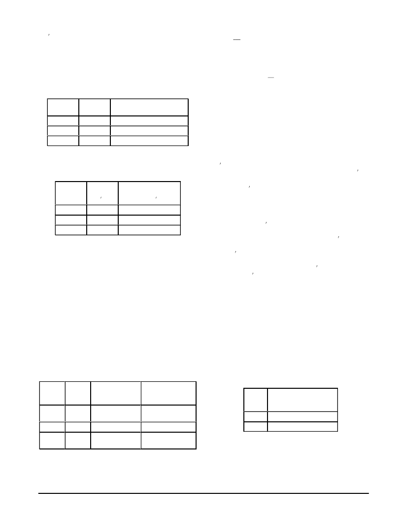
Table 7. Main Phase/Frequency Detector Polarity
áááááááááááááá
á
áááááááááááááá
áááááááááááááá
áááááááááááááá
áá
á
áá
á
(PDout–Lo and PDout–Hi)
ááááááá
á
áááááááááááááá
High
High
Negative
Table 8. Secondary Phase/Frequency
Detector Polarity
ááááááááááááá
á
á
ááááááááááá
ááááááááááááá
ááááááááááááá
ááááááááááááá
áá
Mode Pin
á
á
áá
áá
á
á
(PDout)
ááááá
ááááá
á
á
5B. REFERENCE PINS
Osce and Oscb
Pins 1 and 32 — Reference Oscillator Transistor Emitter
and Base
These pins can be configured to support an external
crystal in a Colpitts oscillator configuration. The required
connections for the crystal circuit are shown in the
Crystal
Oscillator Considerations
section.
Additionally, the pins can be configured to accept an
external reference frequency source, such as a TCXO. In this
case, the reference signal is ac coupled into Osce and the
Oscb pin is left floating. See Figure 11.
Bit C6 and the Mode input pin control the configuration of
these pins per Table 9.
áááááááááááááááá
á
á
áááááááááááááááá
á
ááááááááááá
áá
áá
Low
áááááááááááááááá
Pin
á
Bit C6
áá
á
X
áá
Configuration
ááááá
á
Supports Crystal
ááááá
ááááááá
ááááá
ááááá
Comment
C6 used to control
á
á
áááááááááááááááá
áá
á
ááááá
ááááá
á
5C. LOOP PINS
fin and fin
Pins 12 and 13 — Frequency Input for Main Loop (PLL)
These pins feed the on–chip RF amplifier which drives the
high–speed N counter. This input may be fed differentially.
However, it is usually used in a single–ended configuration
with fin driven while fin is tied to a good RF ground (via a
capacitor). The signal source driving this input must be ac
coupled and originates from an external VCO.
The sensitivity of the RF amplifier is dependent on
frequency as shown in the Loop Specifications table.
Sensitivity of the fin input is specified as a level across a 50
load driven by a 50
source. A VCO that can drive a load
within the data sheet limits can also drive fin. Usually, to avoid
load pull and resultant frequency modulation of the VCO, fin is
lightly coupled by a small value capacitor and/or a resistor.
See the applications circuit of Figure 65.
fin
Pin 30 — Frequency Input for Secondary Loop (PLL )
This pin feeds the on–chip RF amplifier which drives the
high–speed N counter. This input is used in a single–ended
configuration. The signal source driving this input must be ac
coupled and originates from an external VCO.
The sensitivity of the RF amplifier is dependent on
frequency as shown in the Loop Specifications table.
Sensitivity of the fin input is specified as a level across a
50
load driven by a 50
source. A VCO that can drive a
load within the data sheet limits can also drive fin. Usually, to
avoid load pull and resultant frequency modulation of the
VCO, fin is lightly coupled by a small value capacitor and/or
a resistor. See the applications circuit of Figure 65.
If the secondary loop is not used, PLL should be placed in
standby and fin should be left open.
PDout–Hi and PDout–Lo
Pins 19 and 20 — Phase/Frequency Detector Outputs
for Main Loop (PLL)
Each pin is a three–state current source/sink/float output
for use as a loop error signal when combined with an external
low–pass loop filter. Under bit control, PDout–Lo has either
one–quarter or one–eighth the output current of PDout–Hi per
Table 10. The detector is characterized by a linear transfer
function (no dead zone). The polarity of the detector is
controllable. The operation of the detector is described below
and shown in Figure 20.
Table 10. Current Ratio of PDout–Hi
PDout–Hi:PDout–Lo
áááááááááá
á
áááááááááá
áááááááááá
áááááááááá
Bit
á
áááááá
á
When the Mode pin is high, positive polarity occurs when
the Pol pin is low. Also, when the Mode pin is low, polarity
相關(guān)PDF資料 |
PDF描述 |
|---|---|
| MC145230 | Dual PLL Frequency Synthesizers With DACs and Voltage Multipliers(帶DACs和電壓乘法器的雙PLL頻率合成器) |
| MC14528BCL | Dual Monostable Multivibrator |
| MC14528 | DEFLECTION PROCESSOR FOR MULTISYNC MONITORS |
| MC14528 | Dual Monostable Multivibrator |
| MC14528BFEL | Dual Monostable Multivibrator |
相關(guān)代理商/技術(shù)參數(shù) |
參數(shù)描述 |
|---|---|
| MC14522BCP | 制造商:Motorola Inc 功能描述:Counter, Down, Decade, 16 Pin, Plastic, DIP |
| MC14522BDW | 制造商:Motorola Inc 功能描述: |
| MC14526B AC7 WAF | 制造商:ON Semiconductor 功能描述: |
| MC14526BAC7 WAF | 制造商:ON Semiconductor 功能描述: |
| MC14526BCL | 制造商: 功能描述: 制造商:undefined 功能描述: |
發(fā)布緊急采購(gòu),3分鐘左右您將得到回復(fù)。