- 您現(xiàn)在的位置:買賣IC網(wǎng) > PDF目錄371014 > MC145225 (Motorola, Inc.) Dual PLL Frequency Synthesizers With DACs and Voltage Multipliers(帶DACs和電壓乘法器的雙PLL頻率合成器) PDF資料下載
參數(shù)資料
| 型號(hào): | MC145225 |
| 廠商: | Motorola, Inc. |
| 英文描述: | Dual PLL Frequency Synthesizers With DACs and Voltage Multipliers(帶DACs和電壓乘法器的雙PLL頻率合成器) |
| 中文描述: | 雙鎖相環(huán)頻率合成器與DAC和電壓倍增器(帶數(shù)模轉(zhuǎn)換器和電壓乘法器的雙鎖相環(huán)頻率合成器) |
| 文件頁數(shù): | 31/71頁 |
| 文件大小: | 906K |
| 代理商: | MC145225 |
第1頁第2頁第3頁第4頁第5頁第6頁第7頁第8頁第9頁第10頁第11頁第12頁第13頁第14頁第15頁第16頁第17頁第18頁第19頁第20頁第21頁第22頁第23頁第24頁第25頁第26頁第27頁第28頁第29頁第30頁當(dāng)前第31頁第32頁第33頁第34頁第35頁第36頁第37頁第38頁第39頁第40頁第41頁第42頁第43頁第44頁第45頁第46頁第47頁第48頁第49頁第50頁第51頁第52頁第53頁第54頁第55頁第56頁第57頁第58頁第59頁第60頁第61頁第62頁第63頁第64頁第65頁第66頁第67頁第68頁第69頁第70頁第71頁

MC145225 MC145230
31
MOTOROLA RF/IF DEVICE DATA
If we define the damping as resistive, we can define the
opposite or regenerative property as negative resistance.
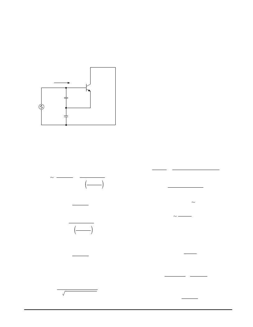
Figure 26 shows the basic circuit of the Colpitts oscillator. C3
has been combined with the crystal elements for simplicity.
For the circuit to oscillate, there must be at least as much
“negative resistance” (regeneration) as there is resistance
(damping). We can define this by deriving the input
impedance for the amplifier.
Figure 26. Colpitts Oscillator Basic Circuit
Q1
C2
C1
Iin
Vin
If a driving signal is defined as Vin, the resultant current
that flows can be identified as Iin. The relationship of Vin to Iin
is
Vin = Iin (Zc1 + Zc2) – Ib (Zc2 –
β
Zc1)
and
0 = Iin (Zc2) + Ib (Zc2 + rb)
where Ib is the base current of transistor Q1. Solving the two
equations and assuming Zc2 << rb, the input impedance can
be expressed as
–gm
ω
2 C1 C2
Zin
j
ω
1
C1 C2
C1 + C2
+
where
ω
= 2
π
f. This is equivalent to the series combination of
a real part whose value is
REAL =
–gm
ω
2 C1 C2
and the imaginary part whose value is
IMAG =
j
ω
1
C1 C2
C1 + C2
To sustain oscillation, the amplifier must generate a
“negative resistance” equal or greater than the REAL part of
the above equation and opposite in polarity.
Rneg =
–gm
ω
2 C1 C2
As long as the relation
–Rneg = –SUM (Rs + Rst + Rc1 + Rc2 + Rc3) ,
the circuit will oscillate and the frequency of oscillation will be
defined as
fo =
2
π
Ls (C1||C2||C3)
1
where C3 is the series frequency adjusting capacitor.
In determining values for C1, C2, and C3, two limits are
considered. At one end is the relationship of C3 to C2 and
C1. If C3 is made 0 or the reactance of C3 is small compared
to the reactance of C1 and C2, no adjustment of the crystal
frequency is possible. The other limit is the relationship
gm Zc1 Zc2 > Rsum
where Rsum is the sum of resistances in the resonant loop.
Since this equation must be true for the circuit to oscillate, it
is obvious that as the values of C1 and C2 are increased, the
series resistances must be reduced and/or gm increased.
Since gm is a function of device current and there is a
physical limit on how small Rsum can be made, at some point
oscillation can no longer be sustained.
Normally, it is desirable to choose the “negative
resistance” to be several times greater than the “damping”
resistance to ensure stable operation. A factor of four or five
is a good “rule of thumb” choice.
To determine crystal power, the equivalent circuit shown in
Figure 27 can be used. In this case, we are addressing a
condition where the transistor amplifier is operating at the
limit of class A; that is, the device is just at cutoff during the
peak negative excursions. At this point,
Re = gm Xc1 Xc2
if the amplitude is constant and the oscillator is stable. For
this to occur, the sum of all resistances in the resonant loop
will be equal to Re, where Re represents the effective
resistance of I1. This can be written as
Rsum = Rs + Rst = Re
where Rs is the crystal resistance and Rst is the additional
distributed resistances within the resonant loop. At the point
where the transistor enters cutoff we have the equation
(Iin – Ib) Zc2+ (Iin +
β
ib) Zc1
=
Xls + Re
β
= current gain of the transistor. Rewriting:
Ib (Zc2 –
β
Zc1)
Zc1 + Zc2 + Xls + Re
For oscillation to occur, we must have
Zc1 + Zc2 + Xls
If we assume
β
Zc1 is normally much greater than Zc2 then
–Ie Zc1
v1 + v2
Xls + Re
–Iin =
.
Iin =
.
0 .
Iin
Re
.
For the condition we have specified,
Ie(bias) + Ie(instantaneous ac) = 0
the transistor is just cutting off and the peak current, Iin is
equal to the bias current. The peak input current is
represented as
Iin(peak) =Ie|Zc1|
Re
.
The power dissipation of the series resistances in the
resonant loop can be written as
Iin(peak)2 R
2
where Rsum = Re.
The power dissipation for the crystal itself becomes
(Ie|Zc1|)2
Pcrystal =
(Ie|Zc1|)2
2 Rsum
=
P =
2 Rs
.
相關(guān)PDF資料 |
PDF描述 |
|---|---|
| MC145230 | Dual PLL Frequency Synthesizers With DACs and Voltage Multipliers(帶DACs和電壓乘法器的雙PLL頻率合成器) |
| MC14528BCL | Dual Monostable Multivibrator |
| MC14528 | DEFLECTION PROCESSOR FOR MULTISYNC MONITORS |
| MC14528 | Dual Monostable Multivibrator |
| MC14528BFEL | Dual Monostable Multivibrator |
相關(guān)代理商/技術(shù)參數(shù) |
參數(shù)描述 |
|---|---|
| MC14522BCP | 制造商:Motorola Inc 功能描述:Counter, Down, Decade, 16 Pin, Plastic, DIP |
| MC14522BDW | 制造商:Motorola Inc 功能描述: |
| MC14526B AC7 WAF | 制造商:ON Semiconductor 功能描述: |
| MC14526BAC7 WAF | 制造商:ON Semiconductor 功能描述: |
| MC14526BCL | 制造商: 功能描述: 制造商:undefined 功能描述: |
發(fā)布緊急采購(gòu),3分鐘左右您將得到回復(fù)。