- 您現(xiàn)在的位置:買賣IC網 > PDF目錄225277 > T431616D-5S (Electronic Theatre Controls, Inc.) 1M x 16 SDRAM 512K x 16bit x 2Banks Synchronous DRAM PDF資料下載
參數資料
| 型號: | T431616D-5S |
| 廠商: | Electronic Theatre Controls, Inc. |
| 英文描述: | 1M x 16 SDRAM 512K x 16bit x 2Banks Synchronous DRAM |
| 中文描述: | 100萬× 16內存為512k × 16Bit的X 2Banks同步DRAM |
| 文件頁數: | 2/74頁 |
| 文件大小: | 781K |
| 代理商: | T431616D-5S |
第1頁當前第2頁第3頁第4頁第5頁第6頁第7頁第8頁第9頁第10頁第11頁第12頁第13頁第14頁第15頁第16頁第17頁第18頁第19頁第20頁第21頁第22頁第23頁第24頁第25頁第26頁第27頁第28頁第29頁第30頁第31頁第32頁第33頁第34頁第35頁第36頁第37頁第38頁第39頁第40頁第41頁第42頁第43頁第44頁第45頁第46頁第47頁第48頁第49頁第50頁第51頁第52頁第53頁第54頁第55頁第56頁第57頁第58頁第59頁第60頁第61頁第62頁第63頁第64頁第65頁第66頁第67頁第68頁第69頁第70頁第71頁第72頁第73頁第74頁
TE
CH
tm
T431616D/E
TM Technology Inc. reserves the right
P. 10
Publication Date: FEB. 2007
to change products or specifications without notice.
Revision: A
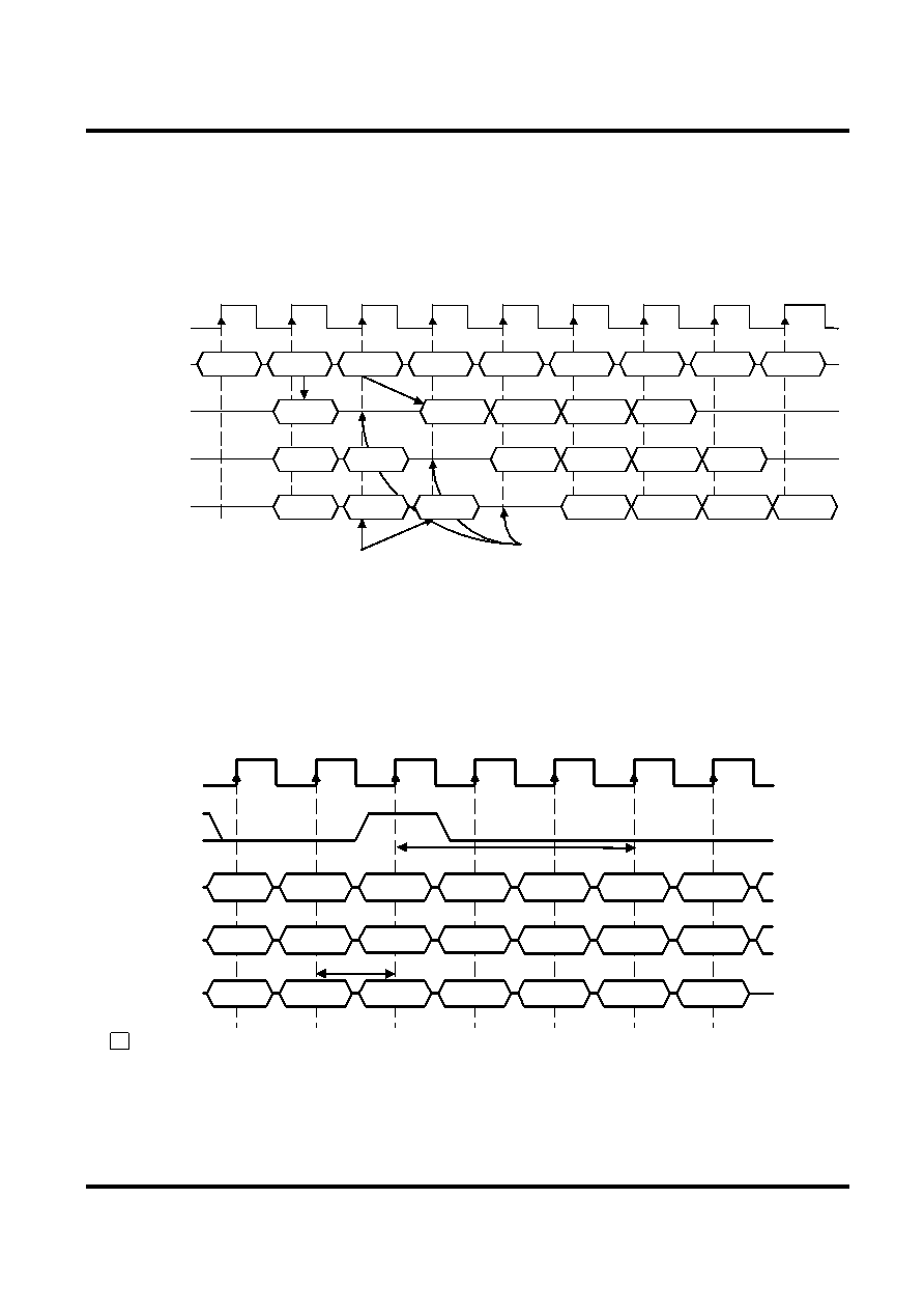
The Read command that interrupts a write burst without auto precharge function should be issued one cycle
after the clock edge in which the last data-in element is registered. In order to avoid data contention, input data
must be removed from the DQs at least one clock cycle before the first read data appears on the outputs (refer to
the following figure). Once the Read command is registered, the data inputs will be ignored and writes will not
be executed.
CLK
COMM AND
T0
T1
T2T3
T4T5
T6T7
T8
DOUT B2
NOP
WRITE A
NOP
READ B
NOP
DIN A0
DOUT B0
DOUT B1
CAS# latency=1
tCK1, DQ's
DOUT B3
don't care
DIN A0
DOUT B2
DOUT B0
DOUT B1
DOUT B3
DIN A0
don't care
DOUT B2
DOUT B0
DOUT B1
DOUT B3
Input data for the write is masked.
Input data must be removedfrom the DQ's at least one clock
cycle before the Read data appears on the outputs to avoid
data contention.
CAS# latency=2
tCK2, DQ's
CAS# latency=3
tCK3, DQ's
Write Interrupted by a Read (Burst Length = 4, CAS# Latency = 1, 2, 3)
The BankPrecharge/PrechargeAll command that interrupts a write burst without the auto precharge function
should be issued m cycles after the clock edge in which the last data-in element is registered, where m equals
tWR/tCK rounded up to the next whole number. In addition, the LDQM/UDQM signals must be used to mask input
data, starting with the clock edge following the last data-in element and ending with the clock edge on which the
BankPrecharge/PrechargeAll command is entered (refer to the following figure).
CLK
T0
T1
T2T3T4T5
T6
WRITE
COMMAND
BANK (S)
ROW
NOP
Precharge
NOP
Activate
BA N K
COL n
DI N
n
DI N
n+ 1
DQM
ADDRESS
DQ
tWR
tRP
: don't care
Note: The LDQM/UDQM can remain low in this example if the length of the write burst is 1 or 2.
Write to Precharge
相關PDF資料 |
PDF描述 |
|---|---|
| T431616D | 1M x 16 SDRAM 512K x 16bit x 2Banks Synchronous DRAM |
| T431616E | 1M x 16 SDRAM 512K x 16bit x 2Banks Synchronous DRAM |
| T450N | 0 MHz - 10000 MHz 50 ohm RF/MICROWAVE TERMINATION |
| T451N | 0 MHz - 10000 MHz 50 ohm RF/MICROWAVE TERMINATION |
| T523-020.00M | TCXO, CLIPPED SINE OUTPUT, 20 MHz |
相關代理商/技術參數 |
參數描述 |
|---|---|
| T431616D-5SG | 制造商:TMT 制造商全稱:TMT 功能描述:1M x 16 SDRAM 512K x 16bit x 2Banks Synchronous DRAM |
| T431616D-6C | 制造商:TMT 制造商全稱:TMT 功能描述:1M x 16 SDRAM 512K x 16bit x 2Banks Synchronous DRAM |
| T431616D-6CG | 制造商:TMT 制造商全稱:TMT 功能描述:1M x 16 SDRAM 512K x 16bit x 2Banks Synchronous DRAM |
| T431616D-6S | 制造商:TMT 制造商全稱:TMT 功能描述:1M x 16 SDRAM 512K x 16bit x 2Banks Synchronous DRAM |
| T431616D-6SG | 制造商:TMT 制造商全稱:TMT 功能描述:1M x 16 SDRAM 512K x 16bit x 2Banks Synchronous DRAM |
發(fā)布緊急采購,3分鐘左右您將得到回復。