- 您現(xiàn)在的位置:買賣IC網(wǎng) > PDF目錄225277 > T431616D-5S (Electronic Theatre Controls, Inc.) 1M x 16 SDRAM 512K x 16bit x 2Banks Synchronous DRAM PDF資料下載
參數(shù)資料
| 型號(hào): | T431616D-5S |
| 廠商: | Electronic Theatre Controls, Inc. |
| 英文描述: | 1M x 16 SDRAM 512K x 16bit x 2Banks Synchronous DRAM |
| 中文描述: | 100萬(wàn)× 16內(nèi)存為512k × 16Bit的X 2Banks同步DRAM |
| 文件頁(yè)數(shù): | 5/74頁(yè) |
| 文件大小: | 781K |
| 代理商: | T431616D-5S |
第1頁(yè)第2頁(yè)第3頁(yè)第4頁(yè)當(dāng)前第5頁(yè)第6頁(yè)第7頁(yè)第8頁(yè)第9頁(yè)第10頁(yè)第11頁(yè)第12頁(yè)第13頁(yè)第14頁(yè)第15頁(yè)第16頁(yè)第17頁(yè)第18頁(yè)第19頁(yè)第20頁(yè)第21頁(yè)第22頁(yè)第23頁(yè)第24頁(yè)第25頁(yè)第26頁(yè)第27頁(yè)第28頁(yè)第29頁(yè)第30頁(yè)第31頁(yè)第32頁(yè)第33頁(yè)第34頁(yè)第35頁(yè)第36頁(yè)第37頁(yè)第38頁(yè)第39頁(yè)第40頁(yè)第41頁(yè)第42頁(yè)第43頁(yè)第44頁(yè)第45頁(yè)第46頁(yè)第47頁(yè)第48頁(yè)第49頁(yè)第50頁(yè)第51頁(yè)第52頁(yè)第53頁(yè)第54頁(yè)第55頁(yè)第56頁(yè)第57頁(yè)第58頁(yè)第59頁(yè)第60頁(yè)第61頁(yè)第62頁(yè)第63頁(yè)第64頁(yè)第65頁(yè)第66頁(yè)第67頁(yè)第68頁(yè)第69頁(yè)第70頁(yè)第71頁(yè)第72頁(yè)第73頁(yè)第74頁(yè)
TE
CH
tm
T431616D/E
TM Technology Inc. reserves the right
P. 13
Publication Date: FEB. 2007
to change products or specifications without notice.
Revision: A
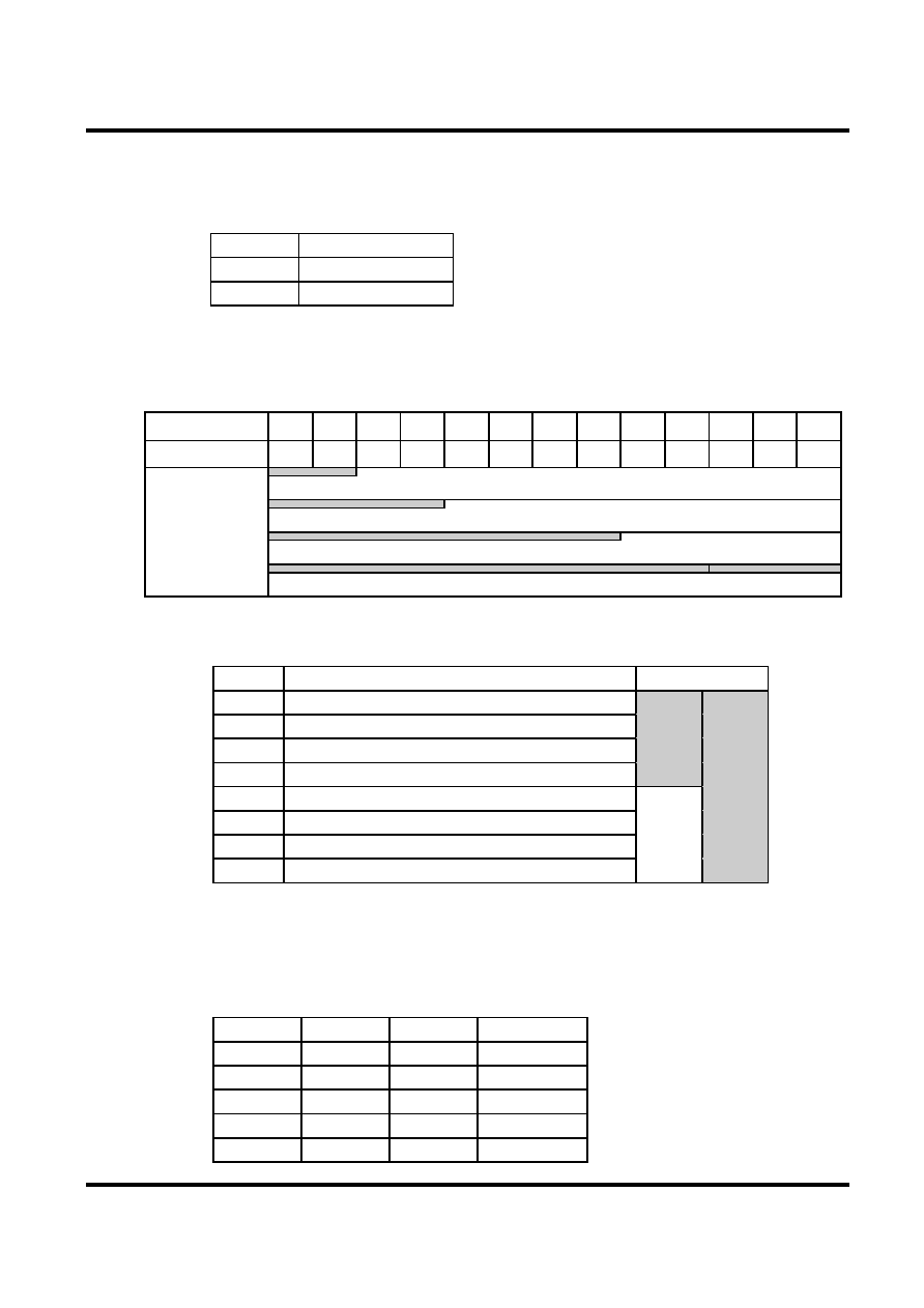
Addressing Mode Select Field (A3)
The Addressing Mode can be one of two modes, Interleave Mode or Sequential Mode. Sequential
Mode supports burst length of 1, 2, 4, 8, or full page, but Interleave Mode only supports burst length
of 4 and 8.
A3
Addressing Mode
0
Sequential
1
Interleave
--- Addressing Sequence of Sequential Mode
An internal column address is performed by increasing the address from the column address which
is input to the device. The internal column address is varied by the Burst Length as shown in the
following table. When the value of column address, (n + m), in the table is larger than 255, only
the least significant 8 bits are effective.
Data n
0
1
2
3
4
5
6
7
-
255
256
257
-
Column Address
n
n+1
n+2
n+3
n+4
n+5
n+6
n+7
-
n+255
n
n+1
-
2 words:
Burst Length
4 words:
8 words:
Full Page: Column address is repeated until terminated.
--- Addressing Sequence of Interleave Mode
A column access is started in the input column address and is performed by inverting the address
bits in the sequence shown in the following table.
Data n
Column Address
Burst Length
Data 0
A7
A6
A5
A4
A3
A2
A1
A0
Data 1
A7
A6
A5
A4
A3
A2
A1
A0#
4 words
Data 2
A7
A6
A5
A4
A3
A2
A1# A0
Data 3
A7
A6
A5
A4
A3
A2
A1# A0#
8 words
Data 4
A7
A6
A5
A4
A3
A2# A1
A0
Data 5
A7
A6
A5
A4
A3
A2# A1
A0#
Data 6
A7
A6
A5
A4
A3
A2# A1# A0
Data 7
A7
A6
A5
A4
A3
A2# A1# A0#
CAS# Latency Field (A6~A4)
This field specifies the number of clock cycles from the assertion of the Read command to the first
read data. The minimum whole value of CAS# Latency depends on the frequency of CLK. The
minimum whole value satisfying the following formula must be programmed into this field.
tCAC(min)
≤ CAS# Latency X tCK
A6
A5
A4
CAS# Latency
0
Reserved
0
1
1 clock
0
1
0
2 clocks
0
1
3 clocks
1
X
Reserved
相關(guān)PDF資料 |
PDF描述 |
|---|---|
| T431616D | 1M x 16 SDRAM 512K x 16bit x 2Banks Synchronous DRAM |
| T431616E | 1M x 16 SDRAM 512K x 16bit x 2Banks Synchronous DRAM |
| T450N | 0 MHz - 10000 MHz 50 ohm RF/MICROWAVE TERMINATION |
| T451N | 0 MHz - 10000 MHz 50 ohm RF/MICROWAVE TERMINATION |
| T523-020.00M | TCXO, CLIPPED SINE OUTPUT, 20 MHz |
相關(guān)代理商/技術(shù)參數(shù) |
參數(shù)描述 |
|---|---|
| T431616D-5SG | 制造商:TMT 制造商全稱:TMT 功能描述:1M x 16 SDRAM 512K x 16bit x 2Banks Synchronous DRAM |
| T431616D-6C | 制造商:TMT 制造商全稱:TMT 功能描述:1M x 16 SDRAM 512K x 16bit x 2Banks Synchronous DRAM |
| T431616D-6CG | 制造商:TMT 制造商全稱:TMT 功能描述:1M x 16 SDRAM 512K x 16bit x 2Banks Synchronous DRAM |
| T431616D-6S | 制造商:TMT 制造商全稱:TMT 功能描述:1M x 16 SDRAM 512K x 16bit x 2Banks Synchronous DRAM |
| T431616D-6SG | 制造商:TMT 制造商全稱:TMT 功能描述:1M x 16 SDRAM 512K x 16bit x 2Banks Synchronous DRAM |
發(fā)布緊急采購(gòu),3分鐘左右您將得到回復(fù)。