- 您現(xiàn)在的位置:買賣IC網(wǎng) > PDF目錄383644 > MT90500 (Mitel Networks Corporation) Multi-Channel ATM AAL1 SAR(多通道 ATM AAL1分段及重組設(shè)備(基于通訊總線的系統(tǒng)與ATM網(wǎng)絡(luò)的接口)) PDF資料下載
參數(shù)資料
| 型號(hào): | MT90500 |
| 廠商: | Mitel Networks Corporation |
| 英文描述: | Multi-Channel ATM AAL1 SAR(多通道 ATM AAL1分段及重組設(shè)備(基于通訊總線的系統(tǒng)與ATM網(wǎng)絡(luò)的接口)) |
| 中文描述: | 多通道自動(dòng)柜員機(jī)AAL1特區(qū)(多通道自動(dòng)柜員機(jī)AAL1分段及重組設(shè)備(基于通訊總線的系統(tǒng)與空中交通管理網(wǎng)絡(luò)的接口)) |
| 文件頁(yè)數(shù): | 74/159頁(yè) |
| 文件大小: | 514K |
| 代理商: | MT90500 |
第1頁(yè)第2頁(yè)第3頁(yè)第4頁(yè)第5頁(yè)第6頁(yè)第7頁(yè)第8頁(yè)第9頁(yè)第10頁(yè)第11頁(yè)第12頁(yè)第13頁(yè)第14頁(yè)第15頁(yè)第16頁(yè)第17頁(yè)第18頁(yè)第19頁(yè)第20頁(yè)第21頁(yè)第22頁(yè)第23頁(yè)第24頁(yè)第25頁(yè)第26頁(yè)第27頁(yè)第28頁(yè)第29頁(yè)第30頁(yè)第31頁(yè)第32頁(yè)第33頁(yè)第34頁(yè)第35頁(yè)第36頁(yè)第37頁(yè)第38頁(yè)第39頁(yè)第40頁(yè)第41頁(yè)第42頁(yè)第43頁(yè)第44頁(yè)第45頁(yè)第46頁(yè)第47頁(yè)第48頁(yè)第49頁(yè)第50頁(yè)第51頁(yè)第52頁(yè)第53頁(yè)第54頁(yè)第55頁(yè)第56頁(yè)第57頁(yè)第58頁(yè)第59頁(yè)第60頁(yè)第61頁(yè)第62頁(yè)第63頁(yè)第64頁(yè)第65頁(yè)第66頁(yè)第67頁(yè)第68頁(yè)第69頁(yè)第70頁(yè)第71頁(yè)第72頁(yè)第73頁(yè)當(dāng)前第74頁(yè)第75頁(yè)第76頁(yè)第77頁(yè)第78頁(yè)第79頁(yè)第80頁(yè)第81頁(yè)第82頁(yè)第83頁(yè)第84頁(yè)第85頁(yè)第86頁(yè)第87頁(yè)第88頁(yè)第89頁(yè)第90頁(yè)第91頁(yè)第92頁(yè)第93頁(yè)第94頁(yè)第95頁(yè)第96頁(yè)第97頁(yè)第98頁(yè)第99頁(yè)第100頁(yè)第101頁(yè)第102頁(yè)第103頁(yè)第104頁(yè)第105頁(yè)第106頁(yè)第107頁(yè)第108頁(yè)第109頁(yè)第110頁(yè)第111頁(yè)第112頁(yè)第113頁(yè)第114頁(yè)第115頁(yè)第116頁(yè)第117頁(yè)第118頁(yè)第119頁(yè)第120頁(yè)第121頁(yè)第122頁(yè)第123頁(yè)第124頁(yè)第125頁(yè)第126頁(yè)第127頁(yè)第128頁(yè)第129頁(yè)第130頁(yè)第131頁(yè)第132頁(yè)第133頁(yè)第134頁(yè)第135頁(yè)第136頁(yè)第137頁(yè)第138頁(yè)第139頁(yè)第140頁(yè)第141頁(yè)第142頁(yè)第143頁(yè)第144頁(yè)第145頁(yè)第146頁(yè)第147頁(yè)第148頁(yè)第149頁(yè)第150頁(yè)第151頁(yè)第152頁(yè)第153頁(yè)第154頁(yè)第155頁(yè)第156頁(yè)第157頁(yè)第158頁(yè)第159頁(yè)
MT90500
74
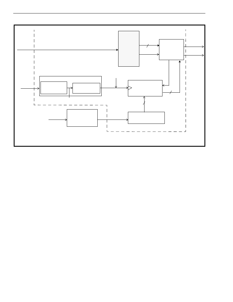
4.6.2.2
Receive SRTS Operation
Note:
The following specification assumes that the MT90500 will perform the SRTS function with the use of
external logic as depicted in Figure 35 and Figure 36.
On the receive side, the MT90500 will generate a local RTS value (EXPECTED_SRTS) as depicted in
Figure 34 (and in a manner identical to that explained in detail in Section 4.6.2.1 for the transmit direction), and
will compare it with the received RTS code (RX_SRTS) from the incoming ATM stream. Up to five locally-
generated RTS values can be stored in a series of internal latches (a 5-deep FIFO).
The MT90500 internal comparator generates a 4-bit complement code that indicates the difference between
the locally generated RTS value and the incoming RTS value (remote - local). The value of this code ranges
from -8 (1000) to +7 (0111). The result of the comparison is then sent out via the SRTSDATA pin, with an
associated strobe output transmitted on SRTSENA. External user logic is necessary to monitor these
difference values, perform the clock adjustment and recover the original ST-BUS clock. If the difference values
increase, it is due to the fact that the remote bus is running faster than the local bus and therefore the local bus
frequency must be increased. Likewise, if the difference values are decreasing, it is because the remote bus is
running more slowly than the local bus, and thus the local bus must be slowed down.
Two 5-deep FIFOs are used to minimize the effect of cell delay variation in the transmission and reception
process and to minimize slips. For both the receive SRTS and the transmit SRTS processes, the FIFOs are
self-aligning: if an underrun or overrun is encountered, the FIFOs’ pointers are re-centered. These errors are
reported in the Clock Module General Status Register at 6082h.
4
Divide by x
4-bit counter
f
nx
MULTIPLE
LATCHES
clk
data_in
Figure 34 - Receive SRTS Operation
FNXI
enable
Byte Counter
CLKx1
period of the RTS
(one 8-cell cycle)
f
B
Gapping Control
f
B
Generator
SRTS Receive Divider Register
4
f
B
= f
S
/ 8 = service byte clock
Comparator
SRTSENA
enable
4
SRTSDATA
RX_SRTS
EXPECTED_
SRTS
RX_SAR
BLOCK
ATM Physical Layer
Network Clock
Internal to MT90500
Receive
ATM Cells
w/ CSI b
its
相關(guān)PDF資料 |
PDF描述 |
|---|---|
| MT90500 | Multi-Channel ATM AAL1 SAR |
| MT90500AL | Multi-Channel ATM AAL1 SAR |
| MT90502 | Multi-Channel AAL2 SAR(多通道 ATM AAL2分段及重組設(shè)備(基于通訊總線的系統(tǒng)與ATM網(wǎng)絡(luò)的接口)) |
| MT90732AP | Ultraframer DS3/E3/DS2/E2/DS1/E1/DS0 |
| MT90732 | Ultraframer DS3/E3/DS2/E2/DS1/E1/DS0 |
相關(guān)代理商/技術(shù)參數(shù) |
參數(shù)描述 |
|---|---|
| MT90500AL | 制造商:MITEL 制造商全稱:Mitel Networks Corporation 功能描述:Multi-Channel ATM AAL1 SAR |
| MT90500AL-ENG1 | 制造商:Mitel Networks Corporation 功能描述: |
| MT90502 | 制造商:ZARLINK 制造商全稱:Zarlink Semiconductor Inc 功能描述:Multi-Channel AAL2 SAR |
| MT90502_06 | 制造商:ZARLINK 制造商全稱:Zarlink Semiconductor Inc 功能描述:Multi-Channel AAL2 SAR |
| MT90502AG | 制造商:Rochester Electronics LLC 功能描述: 制造商:Zarlink Semiconductor Inc 功能描述: |
發(fā)布緊急采購(gòu),3分鐘左右您將得到回復(fù)。