- 您現(xiàn)在的位置:買賣IC網(wǎng) > PDF目錄296800 > PEF22508E (INFINEON TECHNOLOGIES AG) DATACOM, PCM TRANSCEIVER, PBGA256 PDF資料下載
參數(shù)資料
| 型號: | PEF22508E |
| 廠商: | INFINEON TECHNOLOGIES AG |
| 元件分類: | 數(shù)字傳輸電路 |
| 英文描述: | DATACOM, PCM TRANSCEIVER, PBGA256 |
| 封裝: | 17 X 17 MM, 1 MM PITCH, PLASTIC, LBGA-256 |
| 文件頁數(shù): | 176/193頁 |
| 文件大小: | 10683K |
| 代理商: | PEF22508E |
第1頁第2頁第3頁第4頁第5頁第6頁第7頁第8頁第9頁第10頁第11頁第12頁第13頁第14頁第15頁第16頁第17頁第18頁第19頁第20頁第21頁第22頁第23頁第24頁第25頁第26頁第27頁第28頁第29頁第30頁第31頁第32頁第33頁第34頁第35頁第36頁第37頁第38頁第39頁第40頁第41頁第42頁第43頁第44頁第45頁第46頁第47頁第48頁第49頁第50頁第51頁第52頁第53頁第54頁第55頁第56頁第57頁第58頁第59頁第60頁第61頁第62頁第63頁第64頁第65頁第66頁第67頁第68頁第69頁第70頁第71頁第72頁第73頁第74頁第75頁第76頁第77頁第78頁第79頁第80頁第81頁第82頁第83頁第84頁第85頁第86頁第87頁第88頁第89頁第90頁第91頁第92頁第93頁第94頁第95頁第96頁第97頁第98頁第99頁第100頁第101頁第102頁第103頁第104頁第105頁第106頁第107頁第108頁第109頁第110頁第111頁第112頁第113頁第114頁第115頁第116頁第117頁第118頁第119頁第120頁第121頁第122頁第123頁第124頁第125頁第126頁第127頁第128頁第129頁第130頁第131頁第132頁第133頁第134頁第135頁第136頁第137頁第138頁第139頁第140頁第141頁第142頁第143頁第144頁第145頁第146頁第147頁第148頁第149頁第150頁第151頁第152頁第153頁第154頁第155頁第156頁第157頁第158頁第159頁第160頁第161頁第162頁第163頁第164頁第165頁第166頁第167頁第168頁第169頁第170頁第171頁第172頁第173頁第174頁第175頁當(dāng)前第176頁第177頁第178頁第179頁第180頁第181頁第182頁第183頁第184頁第185頁第186頁第187頁第188頁第189頁第190頁第191頁第192頁第193頁
Data Sheet
83
Rev. 1.0, 2005-06-02
OctalLIU
TM
PEF 22508 E
Functional Description
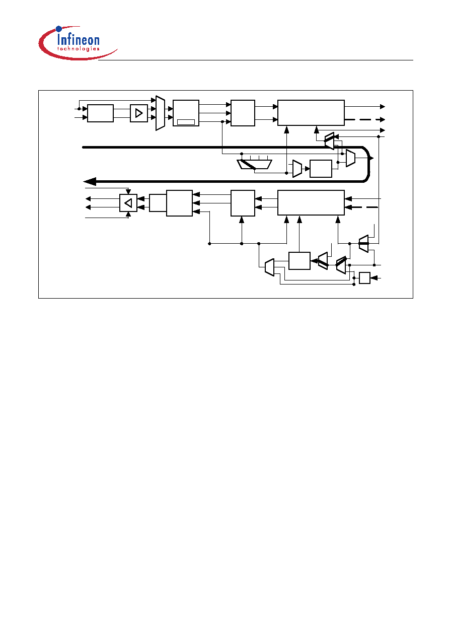
Figure 38
Payload Loop
3.11.6
Alarm Simulation
Alarm simulation does not affect the normal operation of the device. However, possible
real alarm conditions are
not reported to the micro controller or to the remote end when the device is in the alarm simulation mode.
The alarm simulation and setting of the appropriate status bists is initiated by setting the bit MR0.SIM. For details
(differences between E1 and T1/J1 mode) see description in MR0. The following alarms are simulated:
Loss-Of-Signal (LOS)
Alarm Indication Signal (AIS)
Code violation counter (HDB3 Code)
Error counting and indication occurs while this bit is set. After it is reset all simulated error conditions disappear,
but the generated interrupt statuses are still pending until the corresponding interrupt status register is read.
Alarms like AIS and LOS are cleared automatically. Interrupt status registers and error counters are automatically
cleared on read.
3.12
Multi Function Ports
Several signals are available on the multi function ports, see Table 29 and PC1. After reset, input function is
selected (0000
B) with exception of the ports RPC were RCLK output is selected: The register bits PC3.RPC2
have the reset value FH. (Note that PC5.CRP must be set to 1 for an active RCLK output. After reset PC5.CRP
is 0 and RCLK is pulled up.)
Three multi function ports (MFP) for RX - so called as RPA, RPB, RPC - and two MFPs for TX - so called as XPA,
XPB - are implemented for every channel. The port levels are reflected in the appropriate bits of the register MFPI,
see MFPI.
The functions of RPA, RPB and RPC are configured by PC1.RPC1(3:0) , PC2.RPC2(3:0) and PC3.RPC3(3:0)
respectively.The functions of XPA and XPB are configured by PC1.XPC1(3:0) and PC2.XPC2(3:0) respectively.
The actual logical state of the 5 multifunction ports can be read out using the register MFPI. This function together
with static output signal options in Table 29 offers general purpose I/O functionality on unused multi function port
pins.
RCLK
RL1/ROID
RL2
DCO-R
Receive Line
Interface
A
D
C
PayloadLoop
J
internal
receive
clock
Equalizer
Clock &
Data
Recovery
Decoder
RDOP
Dual Receive Elastic Buffer
DPLL
RDON
FCLKR
OctalLIU_payload_loop
Pulse
Shaper,
LBO
Encoder
XDIP
XL2
DCO-X
Dual Transmit Elastic Buffer
Transmit Line
Interface
DAC
XL1
G
H
E
F
%
TCLK
FCLKX
recovered
receive clock
internal
transmit
clock
XL4
XL3
XDIN
相關(guān)PDF資料 |
PDF描述 |
|---|---|
| PEF22554E | DATACOM, FRAMER, PBGA160 |
| PEF22554HT | DATACOM, FRAMER, PQFP144 |
| PES12-42S-N0024 | |
| PESD3V3V4UK,132 | 25 W, UNIDIRECTIONAL, 4 ELEMENT, SILICON, TVS DIODE |
| PF38F3050L0YUQ3A | SPECIALTY MEMORY CIRCUIT, PBGA88 |
相關(guān)代理商/技術(shù)參數(shù) |
參數(shù)描述 |
|---|---|
| PEF22508EV1.1-G | 功能描述:網(wǎng)絡(luò)控制器與處理器 IC T/E RoHS:否 制造商:Micrel 產(chǎn)品:Controller Area Network (CAN) 收發(fā)器數(shù)量: 數(shù)據(jù)速率: 電源電流(最大值):595 mA 最大工作溫度:+ 85 C 安裝風(fēng)格:SMD/SMT 封裝 / 箱體:PBGA-400 封裝:Tray |
| PEF22508EV11G | 制造商:Rochester Electronics LLC 功能描述: 制造商:Infineon Technologies AG 功能描述: |
| PEF22508EV11GXP | 制造商:Lantiq 功能描述:LINE INTERFACE UNITS |
| PEF22508EV11GXT | 制造商:Lantiq 功能描述:LINE INTERFACE UNITS |
| PEF22509EV1.1 | 制造商:Infineon Technologies AG 功能描述:SP000205605_T/E ASIC_TY_PB |
發(fā)布緊急采購,3分鐘左右您將得到回復(fù)。