- 您現(xiàn)在的位置:買賣IC網(wǎng) > PDF目錄300038 > TMX320DM642GNZ500 (TEXAS INSTRUMENTS INC) 64-BIT, 75.19 MHz, OTHER DSP, PBGA548 PDF資料下載
參數(shù)資料
| 型號: | TMX320DM642GNZ500 |
| 廠商: | TEXAS INSTRUMENTS INC |
| 元件分類: | 數(shù)字信號處理 |
| 英文描述: | 64-BIT, 75.19 MHz, OTHER DSP, PBGA548 |
| 封裝: | 27 X 27 MM, 1 MM PITCH, PLASTIC, BGA-548 |
| 文件頁數(shù): | 27/181頁 |
| 文件大?。?/td> | 2291K |
| 代理商: | TMX320DM642GNZ500 |
第1頁第2頁第3頁第4頁第5頁第6頁第7頁第8頁第9頁第10頁第11頁第12頁第13頁第14頁第15頁第16頁第17頁第18頁第19頁第20頁第21頁第22頁第23頁第24頁第25頁第26頁當(dāng)前第27頁第28頁第29頁第30頁第31頁第32頁第33頁第34頁第35頁第36頁第37頁第38頁第39頁第40頁第41頁第42頁第43頁第44頁第45頁第46頁第47頁第48頁第49頁第50頁第51頁第52頁第53頁第54頁第55頁第56頁第57頁第58頁第59頁第60頁第61頁第62頁第63頁第64頁第65頁第66頁第67頁第68頁第69頁第70頁第71頁第72頁第73頁第74頁第75頁第76頁第77頁第78頁第79頁第80頁第81頁第82頁第83頁第84頁第85頁第86頁第87頁第88頁第89頁第90頁第91頁第92頁第93頁第94頁第95頁第96頁第97頁第98頁第99頁第100頁第101頁第102頁第103頁第104頁第105頁第106頁第107頁第108頁第109頁第110頁第111頁第112頁第113頁第114頁第115頁第116頁第117頁第118頁第119頁第120頁第121頁第122頁第123頁第124頁第125頁第126頁第127頁第128頁第129頁第130頁第131頁第132頁第133頁第134頁第135頁第136頁第137頁第138頁第139頁第140頁第141頁第142頁第143頁第144頁第145頁第146頁第147頁第148頁第149頁第150頁第151頁第152頁第153頁第154頁第155頁第156頁第157頁第158頁第159頁第160頁第161頁第162頁第163頁第164頁第165頁第166頁第167頁第168頁第169頁第170頁第171頁第172頁第173頁第174頁第175頁第176頁第177頁第178頁第179頁第180頁第181頁
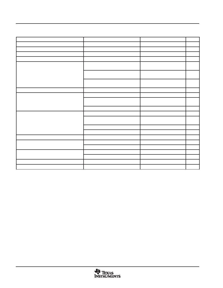
Electrical Specifications
122
July 2002 Revised March 2004
SPRS200E
3.3
Electrical Characteristics Over Recommended Ranges of Supply Voltage and Operating
Case Temperature (Unless Otherwise Noted)
PARAMETER
TEST CONDITIONS
MIN
TYP
MAX
UNIT
VOH
High-level output voltage (except PCI)
DVDD = MIN,
IOH = MAX
2.4
V
VOHP High-level output voltage (PCI)
IOHP = 0.5 mA,
DVDD = 3.3 V
0.9DVDD
V
VOL
Low-level output voltage (except PCI)
DVDD = MIN,
IOL = MAX
0.4
V
VOLP
Low-level output voltage (PCI)
IOLP = 1.5 mA,
DVDD = 3.3 V
0.1DVDD
V
VI = VSS to DVDD no opposing internal
resistor
±10
uA
II
Input current (except PCI)
VI = VSS to DVDD opposing internal
pullup resistor
50
100
150
uA
VI = VSS to DVDD opposing internal
pulldown resistor
150
100
50
uA
IIP
Input leakage current (PCI)§
0 < VIP < DVDD = 3.3 V
±10
uA
EMIF, CLKOUT4, CLKOUT6, EMUx
16
mA
IOH
High-level output current
Video Ports, Timer, TDO, GPIO
(Excluding GP0[15:9, 2, 1]), McBSP
8
mA
PCI/HPI
0.5
mA
EMIF, CLKOUT4, CLKOUT6, EMUx
16
mA
IOL
Low-level output current
Video Ports, Timer, TDO, GPIO
(Excluding GP0[15:9, 2, 1]), McBSP
8
mA
IOL
Low-level output current
SCL0 and SDA0
3
mA
PCI/HPI
1.5
mA
IOZ
Off-state output current
VO = DVDD or 0 V
±10
uA
ICDD
Core supply current#
CVDD = 1.4 V, CPU clock = 600 MHz
793
mA
ICDD
Core supply current#
CVDD = 1.2 V, CPU clock = 500 MHz
555
mA
IDDD
I/O supply current#
DVDD = 3.3 V, CPU clock = 600 MHz
165
mA
IDDD
I/O supply current#
DVDD = 3.3 V, CPU clock = 500 MHz
135
mA
Ci
Input capacitance
10
pF
Co
Output capacitance
10
pF
For test conditions shown as MIN, MAX, or NOM, use the appropriate value specified in the recommended operating conditions table.
Applies only to pins with an internal pullup (IPU) or pulldown (IPD) resistor.
§ PCI input leakage currents include Hi-Z output leakage for all bidirectional buffers with 3-state outputs.
These rated numbers are from the PCI specification version 2.3. The DC specification and AC specification are defined in Tables 4-3 and 4-4,
respectively.
# Measured with average activity (50% high/50% low power) at 25°C case temperature and 133-MHz EMIF for -600 speed (100-MHz EMIF for
-500 speed). This model represents a device performing high-DSP-activity operations 50% of the time, and the remainder performing
low-DSP-activity operations. The high/low-DSP-activity models are defined as follows:
High-DSP-Activity Model:
CPU: 8 instructions/cycle with 2 LDDW instructions [L1 Data Memory: 128 bits/cycle via LDDW instructions;
L1 Program Memory: 256 bits/cycle; L2/EMIF EDMA: 50% writes, 50% reads to/from SDRAM (50% bit-switching)]
McBSP: 2 channels at E1 rate
Timers: 2 timers at maximum rate
Low-DSP-Activity Model:
CPU: 2 instructions/cycle with 1 LDH instruction [L1 Data Memory: 16 bits/cycle; L1 Program Memory: 256 bits per 4 cycles;
L2/EMIF EDMA: None]
McBSP: 2 channels at E1 rate
Timers: 2 timers at maximum rate
The actual current draw is highly application-dependent. For more details on core and I/O activity, refer to the TMS320DMx Power Consumption
Summary application report (literature number SPRA962).
3.4
Recommended Clock and Control Signal Transition Behavior
All clocks and control signals must transition between VIH and VIL (or between VIL and VIH) in a monotonic
manner.
ADV
ANCE
INFORMA
TION
相關(guān)PDF資料 |
PDF描述 |
|---|---|
| TN4002PM | 10 MHz - 500 MHz RF/MICROWAVE WIDE BAND LOW POWER AMPLIFIER |
| TN5171PM | 20 MHz - 150 MHz RF/MICROWAVE WIDE BAND MEDIUM POWER AMPLIFIER |
| TOCP172-1MB | 970/1000 um, MULTI MODE, SIMPLEX FIBER OPTIC CONNECTOR |
| TOCP172-20CB | 970/1000 um, MULTI MODE, SIMPLEX FIBER OPTIC CONNECTOR |
| TOD5202FE | Optoelectronic |
相關(guān)代理商/技術(shù)參數(shù) |
參數(shù)描述 |
|---|---|
| TMX320DM6435AZDU | 制造商:Texas Instruments 功能描述: |
| TMX320DM6437AZDUA | 功能描述:開發(fā)板和工具包 - TMS320 Digl Media Processor RoHS:否 制造商:Texas Instruments 產(chǎn)品:Experimenter Kits 工具用于評估:F2802x 核心:TMS320 接口類型:UART, USB 工作電源電壓: |
| TMX320DM6437AZWTA | 制造商:Texas Instruments 功能描述:TMX320DM6437 PG1.1 361PIN PB-FREE NFBGA - Trays |
| TMX320DM6437BZDUA | 功能描述:數(shù)字信號處理器和控制器 - DSP, DSC Dig Media Processor RoHS:否 制造商:Microchip Technology 核心:dsPIC 數(shù)據(jù)總線寬度:16 bit 程序存儲器大小:16 KB 數(shù)據(jù) RAM 大小:2 KB 最大時鐘頻率:40 MHz 可編程輸入/輸出端數(shù)量:35 定時器數(shù)量:3 設(shè)備每秒兆指令數(shù):50 MIPs 工作電源電壓:3.3 V 最大工作溫度:+ 85 C 封裝 / 箱體:TQFP-44 安裝風(fēng)格:SMD/SMT |
| TMX320DM6437BZWTA | 功能描述:數(shù)字信號處理器和控制器 - DSP, DSC Dig Media Processor RoHS:否 制造商:Microchip Technology 核心:dsPIC 數(shù)據(jù)總線寬度:16 bit 程序存儲器大小:16 KB 數(shù)據(jù) RAM 大小:2 KB 最大時鐘頻率:40 MHz 可編程輸入/輸出端數(shù)量:35 定時器數(shù)量:3 設(shè)備每秒兆指令數(shù):50 MIPs 工作電源電壓:3.3 V 最大工作溫度:+ 85 C 封裝 / 箱體:TQFP-44 安裝風(fēng)格:SMD/SMT |
發(fā)布緊急采購,3分鐘左右您將得到回復(fù)。