- 您現(xiàn)在的位置:買(mǎi)賣(mài)IC網(wǎng) > PDF目錄300038 > TMX320DM642GNZ500 (TEXAS INSTRUMENTS INC) 64-BIT, 75.19 MHz, OTHER DSP, PBGA548 PDF資料下載
參數(shù)資料
| 型號(hào): | TMX320DM642GNZ500 |
| 廠商: | TEXAS INSTRUMENTS INC |
| 元件分類: | 數(shù)字信號(hào)處理 |
| 英文描述: | 64-BIT, 75.19 MHz, OTHER DSP, PBGA548 |
| 封裝: | 27 X 27 MM, 1 MM PITCH, PLASTIC, BGA-548 |
| 文件頁(yè)數(shù): | 51/181頁(yè) |
| 文件大?。?/td> | 2291K |
| 代理商: | TMX320DM642GNZ500 |
第1頁(yè)第2頁(yè)第3頁(yè)第4頁(yè)第5頁(yè)第6頁(yè)第7頁(yè)第8頁(yè)第9頁(yè)第10頁(yè)第11頁(yè)第12頁(yè)第13頁(yè)第14頁(yè)第15頁(yè)第16頁(yè)第17頁(yè)第18頁(yè)第19頁(yè)第20頁(yè)第21頁(yè)第22頁(yè)第23頁(yè)第24頁(yè)第25頁(yè)第26頁(yè)第27頁(yè)第28頁(yè)第29頁(yè)第30頁(yè)第31頁(yè)第32頁(yè)第33頁(yè)第34頁(yè)第35頁(yè)第36頁(yè)第37頁(yè)第38頁(yè)第39頁(yè)第40頁(yè)第41頁(yè)第42頁(yè)第43頁(yè)第44頁(yè)第45頁(yè)第46頁(yè)第47頁(yè)第48頁(yè)第49頁(yè)第50頁(yè)當(dāng)前第51頁(yè)第52頁(yè)第53頁(yè)第54頁(yè)第55頁(yè)第56頁(yè)第57頁(yè)第58頁(yè)第59頁(yè)第60頁(yè)第61頁(yè)第62頁(yè)第63頁(yè)第64頁(yè)第65頁(yè)第66頁(yè)第67頁(yè)第68頁(yè)第69頁(yè)第70頁(yè)第71頁(yè)第72頁(yè)第73頁(yè)第74頁(yè)第75頁(yè)第76頁(yè)第77頁(yè)第78頁(yè)第79頁(yè)第80頁(yè)第81頁(yè)第82頁(yè)第83頁(yè)第84頁(yè)第85頁(yè)第86頁(yè)第87頁(yè)第88頁(yè)第89頁(yè)第90頁(yè)第91頁(yè)第92頁(yè)第93頁(yè)第94頁(yè)第95頁(yè)第96頁(yè)第97頁(yè)第98頁(yè)第99頁(yè)第100頁(yè)第101頁(yè)第102頁(yè)第103頁(yè)第104頁(yè)第105頁(yè)第106頁(yè)第107頁(yè)第108頁(yè)第109頁(yè)第110頁(yè)第111頁(yè)第112頁(yè)第113頁(yè)第114頁(yè)第115頁(yè)第116頁(yè)第117頁(yè)第118頁(yè)第119頁(yè)第120頁(yè)第121頁(yè)第122頁(yè)第123頁(yè)第124頁(yè)第125頁(yè)第126頁(yè)第127頁(yè)第128頁(yè)第129頁(yè)第130頁(yè)第131頁(yè)第132頁(yè)第133頁(yè)第134頁(yè)第135頁(yè)第136頁(yè)第137頁(yè)第138頁(yè)第139頁(yè)第140頁(yè)第141頁(yè)第142頁(yè)第143頁(yè)第144頁(yè)第145頁(yè)第146頁(yè)第147頁(yè)第148頁(yè)第149頁(yè)第150頁(yè)第151頁(yè)第152頁(yè)第153頁(yè)第154頁(yè)第155頁(yè)第156頁(yè)第157頁(yè)第158頁(yè)第159頁(yè)第160頁(yè)第161頁(yè)第162頁(yè)第163頁(yè)第164頁(yè)第165頁(yè)第166頁(yè)第167頁(yè)第168頁(yè)第169頁(yè)第170頁(yè)第171頁(yè)第172頁(yè)第173頁(yè)第174頁(yè)第175頁(yè)第176頁(yè)第177頁(yè)第178頁(yè)第179頁(yè)第180頁(yè)第181頁(yè)
Reset Timing
144
July 2002 Revised March 2004
SPRS200E
5.7
Reset Timing
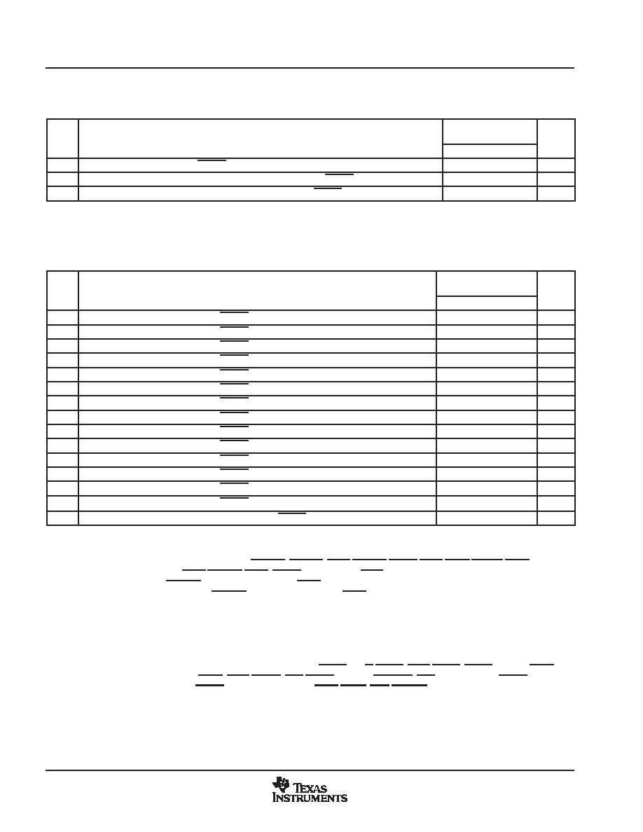
Table 517. Timing Requirements for Reset (see Figure 522)
NO.
500
600
UNIT
NO.
MIN
MAX
UNIT
1
tw(RST)
Width of the RESET pulse
250
s
16
tsu(boot)
Setup time, boot configuration bits valid before RESET high
4E or 4C
ns
17
th(boot)
Hold time, boot configuration bits valid after RESET high
4E or 4C
ns
AEA[22:19], LENDIAN, PCIEEAI, and HD5/AD5 are the boot configuration pins during device reset.
E = 1/AECLKIN clock frequency in ns. C = 1/CLKIN clock frequency in ns.
Select the MIN parameter value, whichever value is larger.
Table 518. Switching Characteristics Over Recommended Operating Conditions During Reset§||
(see Figure 522)
NO.
PARAMETER
500
600
UNIT
NO.
PARAMETER
MIN
MAX
UNIT
2
td(RSTL-ECKI)
Delay time, RESET low to AECLKIN synchronized internally
2E
3P + 20E
ns
3
td(RSTH-ECKI)
Delay time, RESET high to AECLKIN synchronized internally
2E
8P + 20E
ns
4
td(RSTL-ECKO1HZ)
Delay time, RESET low to AECLKOUT1 high impedance
2E
ns
5
td(RSTH-ECKO1V)
Delay time, RESET high to AECLKOUT1 valid
8P + 20E
ns
6
td(RSTL-EMIFZHZ)
Delay time, RESET low to EMIF Z high impedance
2E
3P + 4E
ns
7
td(RSTH-EMIFZV)
Delay time, RESET high to EMIF Z valid
16E
8P + 20E
ns
8
td(RSTL-EMIFHIV)
Delay time, RESET low to EMIF high group invalid
2E
ns
9
td(RSTH-EMIFHV)
Delay time, RESET high to EMIF high group valid
8P + 20E
ns
10
td(RSTL-EMIFLIV)
Delay time, RESET low to EMIF low group invalid
2E
ns
11
td(RSTH-EMIFLV)
Delay time, RESET high to EMIF low group valid
8P + 20E
ns
12
td(RSTL-LOWIV)
Delay time, RESET low to low group invalid
0
ns
13
td(RSTH-LOWV)
Delay time, RESET high to low group valid
11P
ns
14
td(RSTL-ZHZ)
Delay time, RESET low to Z group high impedance
0
ns
15
td(RSTH-ZV)
Delay time, RESET high to Z group valid
2P
8P
ns
18
td(PCLK-RSTH)
Delay time, PCLK active to RESET high#
32N
ns
§ P = 1/CPU clock frequency in ns. For example, when running parts at 600 MHz, use P = 1.67 ns.
E = the EMIF input clock (AECLKIN, CPU/4 clock, or CPU/6 clock) period in ns for EMIFA.
# N = the PCI input clock (PCLK) period in ns. When PCI is enabled (PCI_EN = 1), this parameter must be met.
|| EMIF Z group consists of:
AEA[22:3], AED[63:0], ACE[3:0], ABE[7:0], AARE/ASDCAS/ASADS/ASRE,AAWE/ASDWE/ASWE,
and AAOE/ASDRAS/ASOE, ASOE3, ASDCKE, and APDT.
EMIF high group consists of: AHOLDA (when the corresponding HOLD input is high)
EMIF low group consists of:
ABUSREQ; AHOLDA (when the corresponding HOLD input is low)
Low group consists of:
XSP_CS, XSP_CLK/MDCLK, and XSP_DO/MDIO; all of which apply only when PCI EEPROM is enabled
(with PCI_EN = 1 and MCBSP2_EN = 0). Otherwise, the CLKX2/XSP_CLK and DX2/XSP_DO pins are in the
Z group. For more details on the PCI configuration pins, see the Device Configurations section of this data sheet.
Z group consists of:
HD[31:0]/AD[31:0] and the muxed EMAC output pins, XSP_CLK/MDCLK, XSP_DO/MDIO, VP0D[2]/CLKX0,
VP1D[2]/CLKX1, VP0D[3]/FSX0, VP1D[3]/FSX1, VP0D[4]/DX0, VP1D[4]/DX1, VP0D[8]/CLKR0,
VP1D[8]/CLKR1, VP0D[7]/FSR0, VP1D[7]/FSR1, TOUT0, TOUT1,
VDAC/GP0[8]/PCI66, GP0[7:0], GP0[10]/PCBE3, HR/W/PCBE2, HDS2/PCBE1, PCBE0, GP0[13]/PINTA,
GP0[11]/PREQ, HDS1/PSERR, HCS/PPERR, HCNTL1/PDEVSEL, HAS/PPAR, HCNTL0/PSTOP,
HHWIL/PTRDY (16-bit HPI mode only), HRDY/PIRDY, HINT/PFRAME, VP0D[19:9, 6,5,1,0],
VP1D[19:9, 6,5,1,0], and VP2D[19:0].
ADV
ANCE
INFORMA
TION
相關(guān)PDF資料 |
PDF描述 |
|---|---|
| TN4002PM | 10 MHz - 500 MHz RF/MICROWAVE WIDE BAND LOW POWER AMPLIFIER |
| TN5171PM | 20 MHz - 150 MHz RF/MICROWAVE WIDE BAND MEDIUM POWER AMPLIFIER |
| TOCP172-1MB | 970/1000 um, MULTI MODE, SIMPLEX FIBER OPTIC CONNECTOR |
| TOCP172-20CB | 970/1000 um, MULTI MODE, SIMPLEX FIBER OPTIC CONNECTOR |
| TOD5202FE | Optoelectronic |
相關(guān)代理商/技術(shù)參數(shù) |
參數(shù)描述 |
|---|---|
| TMX320DM6435AZDU | 制造商:Texas Instruments 功能描述: |
| TMX320DM6437AZDUA | 功能描述:開(kāi)發(fā)板和工具包 - TMS320 Digl Media Processor RoHS:否 制造商:Texas Instruments 產(chǎn)品:Experimenter Kits 工具用于評(píng)估:F2802x 核心:TMS320 接口類型:UART, USB 工作電源電壓: |
| TMX320DM6437AZWTA | 制造商:Texas Instruments 功能描述:TMX320DM6437 PG1.1 361PIN PB-FREE NFBGA - Trays |
| TMX320DM6437BZDUA | 功能描述:數(shù)字信號(hào)處理器和控制器 - DSP, DSC Dig Media Processor RoHS:否 制造商:Microchip Technology 核心:dsPIC 數(shù)據(jù)總線寬度:16 bit 程序存儲(chǔ)器大小:16 KB 數(shù)據(jù) RAM 大小:2 KB 最大時(shí)鐘頻率:40 MHz 可編程輸入/輸出端數(shù)量:35 定時(shí)器數(shù)量:3 設(shè)備每秒兆指令數(shù):50 MIPs 工作電源電壓:3.3 V 最大工作溫度:+ 85 C 封裝 / 箱體:TQFP-44 安裝風(fēng)格:SMD/SMT |
| TMX320DM6437BZWTA | 功能描述:數(shù)字信號(hào)處理器和控制器 - DSP, DSC Dig Media Processor RoHS:否 制造商:Microchip Technology 核心:dsPIC 數(shù)據(jù)總線寬度:16 bit 程序存儲(chǔ)器大小:16 KB 數(shù)據(jù) RAM 大小:2 KB 最大時(shí)鐘頻率:40 MHz 可編程輸入/輸出端數(shù)量:35 定時(shí)器數(shù)量:3 設(shè)備每秒兆指令數(shù):50 MIPs 工作電源電壓:3.3 V 最大工作溫度:+ 85 C 封裝 / 箱體:TQFP-44 安裝風(fēng)格:SMD/SMT |
發(fā)布緊急采購(gòu),3分鐘左右您將得到回復(fù)。