- 您現(xiàn)在的位置:買賣IC網(wǎng) > PDF目錄1973 > XC3SD1800A-4CSG484LI (Xilinx Inc)IC FPGA SPARTAN 3 DSP 484CSGBGA PDF資料下載
參數(shù)資料
| 型號(hào): | XC3SD1800A-4CSG484LI |
| 廠商: | Xilinx Inc |
| 文件頁(yè)數(shù): | 53/101頁(yè) |
| 文件大?。?/td> | 0K |
| 描述: | IC FPGA SPARTAN 3 DSP 484CSGBGA |
| 標(biāo)準(zhǔn)包裝: | 84 |
| 系列: | Spartan®-3A DSP |
| LAB/CLB數(shù): | 4160 |
| 邏輯元件/單元數(shù): | 37440 |
| RAM 位總計(jì): | 1548288 |
| 輸入/輸出數(shù): | 309 |
| 門數(shù): | 1800000 |
| 電源電壓: | 1.14 V ~ 1.26 V |
| 安裝類型: | 表面貼裝 |
| 工作溫度: | -40°C ~ 100°C |
| 封裝/外殼: | 484-FBGA,CSPBGA |
| 供應(yīng)商設(shè)備封裝: | 484-CSPBGA |
第1頁(yè)第2頁(yè)第3頁(yè)第4頁(yè)第5頁(yè)第6頁(yè)第7頁(yè)第8頁(yè)第9頁(yè)第10頁(yè)第11頁(yè)第12頁(yè)第13頁(yè)第14頁(yè)第15頁(yè)第16頁(yè)第17頁(yè)第18頁(yè)第19頁(yè)第20頁(yè)第21頁(yè)第22頁(yè)第23頁(yè)第24頁(yè)第25頁(yè)第26頁(yè)第27頁(yè)第28頁(yè)第29頁(yè)第30頁(yè)第31頁(yè)第32頁(yè)第33頁(yè)第34頁(yè)第35頁(yè)第36頁(yè)第37頁(yè)第38頁(yè)第39頁(yè)第40頁(yè)第41頁(yè)第42頁(yè)第43頁(yè)第44頁(yè)第45頁(yè)第46頁(yè)第47頁(yè)第48頁(yè)第49頁(yè)第50頁(yè)第51頁(yè)第52頁(yè)當(dāng)前第53頁(yè)第54頁(yè)第55頁(yè)第56頁(yè)第57頁(yè)第58頁(yè)第59頁(yè)第60頁(yè)第61頁(yè)第62頁(yè)第63頁(yè)第64頁(yè)第65頁(yè)第66頁(yè)第67頁(yè)第68頁(yè)第69頁(yè)第70頁(yè)第71頁(yè)第72頁(yè)第73頁(yè)第74頁(yè)第75頁(yè)第76頁(yè)第77頁(yè)第78頁(yè)第79頁(yè)第80頁(yè)第81頁(yè)第82頁(yè)第83頁(yè)第84頁(yè)第85頁(yè)第86頁(yè)第87頁(yè)第88頁(yè)第89頁(yè)第90頁(yè)第91頁(yè)第92頁(yè)第93頁(yè)第94頁(yè)第95頁(yè)第96頁(yè)第97頁(yè)第98頁(yè)第99頁(yè)第100頁(yè)第101頁(yè)
Spartan-3A DSP FPGA Family: DC and Switching Characteristics
DS610 (v3.0) October 4, 2010
Product Specification
55
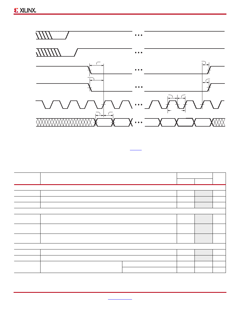
Slave Parallel Mode Timing
X-Ref Target - Figure 12
Figure 12: Waveforms for Slave Parallel Configuration
Table 51: Timing for the Slave Parallel Configuration Mode
Symbol
Description
All Speed Grades
Units
Min
Max
Setup Times
The time from the setup of data at the D0-D7 pins to the rising transition at the CCLK pin
7
–ns
TSMCSCC
Setup time on the CSI_B pin before the rising transition at the CCLK pin
7
–ns
TSMCCW
Setup time on the RDWR_B pin before the rising transition at the CCLK pin
17
–ns
Hold Times
TSMCCD
The time from the rising transition at the CCLK pin to the point when data is last held at
the D0-D7 pins
1
–ns
TSMCCCS
The time from the rising transition at the CCLK pin to the point when a logic level is last
held at the CSO_B pin
0
–ns
TSMWCC
The time from the rising transition at the CCLK pin to the point when a logic level is last
held at the RDWR_B pin
0
–ns
Clock Timing
TCCH
The High pulse width at the CCLK input pin
5
–ns
TCCL
The Low pulse width at the CCLK input pin
5
–ns
FCCPAR
Frequency of the clock signal at the CCLK input pin No bitstream compression
0
80
MHz
With bitstream compression
0
80
MHz
Notes:
1.
The numbers in this table are based on the operating conditions set forth in Table 7.
2.
Some Xilinx documents refer to Parallel modes as “SelectMAP” modes.
DS529-3_02_051607
Byte 0
Byte 1
Byte n
Byte n+1
T
SMWCC
1/F
CCPAR
T
SMCCCS
T
SCCH
T
SMCCW
T
SMCCD
T
SMCSCC
T
SMDCC
PROG_B
(Input)
(Open-Drain)
INIT_B
(Input)
CSI_B
RDWR_B
(Input)
CCLK
(Inputs)
D0 - D7
T
MCCH
T
SCCL
T
MCCL
Notes:
1.
It is possible to abort configuration by pulling CSI_B Low in a given CCLK cycle, then switching RDWR_B Low or High in any subsequent
cycle for which CSI_B remains Low. The RDWR_B pin asynchronously controls the driver impedance of the D0–D7 bus. When RDWR_B
switches High, be careful to avoid contention on the D0–D7 bus.
2.
To pause configuration, pause CCLK instead of de-asserting CSI_B. See UG332, Chapter 7, section “Non-Continuous SelectMAP Data
Loading” for more details.
相關(guān)PDF資料 |
PDF描述 |
|---|---|
| XC3SD3400A-4FGG676I | SPARTAN-3ADSP FPGA 3400K 676FBGA |
| XC4036XLA-09HQ240C | IC FPGA C 2.5V 288 I/O 240HQFP |
| XC4062XL-09HQ240C | IC FPGA C-TEMP 3.3V 240-HQFP |
| XC4085XL-3BG560I | IC FPGA I-TEMP 3.3V 3SPD 560MBGA |
| XC4VLX100-10FFG1513C | IC FPGA VIRTEX-4 100K 1513-FBGA |
相關(guān)代理商/技術(shù)參數(shù) |
參數(shù)描述 |
|---|---|
| XC3SD1800A-4FG676C | 制造商:Xilinx 功能描述:FPGA SPARTAN-3A 1.8M GATES 37440 CELLS 667MHZ 1.2V 676FBGA - Trays 制造商:Xilinx 功能描述:IC FPGA 519 I/O 676FBGA 制造商:Xilinx 功能描述:SPARTAN-3ADSP FPGA 1800K 676FBGA |
| XC3SD1800A-4FG676I | 功能描述:SPARTAN-3ADSP FPGA 1800K 676FBGA RoHS:否 類別:集成電路 (IC) >> 嵌入式 - FPGA(現(xiàn)場(chǎng)可編程門陣列) 系列:Spartan®-3A DSP 標(biāo)準(zhǔn)包裝:40 系列:Spartan® 6 LX LAB/CLB數(shù):3411 邏輯元件/單元數(shù):43661 RAM 位總計(jì):2138112 輸入/輸出數(shù):358 門數(shù):- 電源電壓:1.14 V ~ 1.26 V 安裝類型:表面貼裝 工作溫度:-40°C ~ 100°C 封裝/外殼:676-BGA 供應(yīng)商設(shè)備封裝:676-FBGA(27x27) |
| XC3SD1800A-4FGG676C | 功能描述:SPARTAN-3ADSP FPGA 1800K 676FBGA RoHS:是 類別:集成電路 (IC) >> 嵌入式 - FPGA(現(xiàn)場(chǎng)可編程門陣列) 系列:Spartan®-3A DSP 標(biāo)準(zhǔn)包裝:24 系列:ECP2 LAB/CLB數(shù):1500 邏輯元件/單元數(shù):12000 RAM 位總計(jì):226304 輸入/輸出數(shù):131 門數(shù):- 電源電壓:1.14 V ~ 1.26 V 安裝類型:表面貼裝 工作溫度:0°C ~ 85°C 封裝/外殼:208-BFQFP 供應(yīng)商設(shè)備封裝:208-PQFP(28x28) |
| XC3SD1800A-4FGG676CES | 制造商:Xilinx 功能描述: |
| XC3SD1800A-4FGG676I | 功能描述:SPARTAN-3ADSP FPGA 1800K 676FBGA RoHS:是 類別:集成電路 (IC) >> 嵌入式 - FPGA(現(xiàn)場(chǎng)可編程門陣列) 系列:Spartan®-3A DSP 標(biāo)準(zhǔn)包裝:40 系列:Spartan® 6 LX LAB/CLB數(shù):3411 邏輯元件/單元數(shù):43661 RAM 位總計(jì):2138112 輸入/輸出數(shù):358 門數(shù):- 電源電壓:1.14 V ~ 1.26 V 安裝類型:表面貼裝 工作溫度:-40°C ~ 100°C 封裝/外殼:676-BGA 供應(yīng)商設(shè)備封裝:676-FBGA(27x27) |
發(fā)布緊急采購(gòu),3分鐘左右您將得到回復(fù)。