- 您現(xiàn)在的位置:買賣IC網(wǎng) > PDF目錄377488 > IDT88P8344BHGI (INTEGRATED DEVICE TECHNOLOGY INC) SPI EXCHANGE 4 x SPI-3 TO SPI-4 Issue 1.0 PDF資料下載
參數(shù)資料
| 型號: | IDT88P8344BHGI |
| 廠商: | INTEGRATED DEVICE TECHNOLOGY INC |
| 元件分類: | 微控制器/微處理器 |
| 英文描述: | SPI EXCHANGE 4 x SPI-3 TO SPI-4 Issue 1.0 |
| 中文描述: | SPECIALTY MICROPROCESSOR CIRCUIT, PBGA820 |
| 封裝: | GREEN, PLASTIC, BGA-820 |
| 文件頁數(shù): | 44/98頁 |
| 文件大?。?/td> | 601K |
| 代理商: | IDT88P8344BHGI |
第1頁第2頁第3頁第4頁第5頁第6頁第7頁第8頁第9頁第10頁第11頁第12頁第13頁第14頁第15頁第16頁第17頁第18頁第19頁第20頁第21頁第22頁第23頁第24頁第25頁第26頁第27頁第28頁第29頁第30頁第31頁第32頁第33頁第34頁第35頁第36頁第37頁第38頁第39頁第40頁第41頁第42頁第43頁當前第44頁第45頁第46頁第47頁第48頁第49頁第50頁第51頁第52頁第53頁第54頁第55頁第56頁第57頁第58頁第59頁第60頁第61頁第62頁第63頁第64頁第65頁第66頁第67頁第68頁第69頁第70頁第71頁第72頁第73頁第74頁第75頁第76頁第77頁第78頁第79頁第80頁第81頁第82頁第83頁第84頁第85頁第86頁第87頁第88頁第89頁第90頁第91頁第92頁第93頁第94頁第95頁第96頁第97頁第98頁
44
IDT88P8344 SPI EXCHANGE 4 x SPI-3 TO SPI-4
INDUSTRIAL TEMPERATURE RANGE
APRIL 10, 2006
example, a SPI-4 clock of 400 MHz gives a data unit interval of 1.25 ns, so match
the lengths within the entire signal group to within 625 ps, or 3 inches.
3) Keep P and N signals within a differential pair on the same layer with the
mnimumtrace spacing possible while still being able to get 100 ohms differential
impedance (tightly edge-coupled pair routing).
4) Route all differential pairs as 100 Ohmembedded differential stripline (on
an inner layer, referencing ground planes). For example, 7 ml wide 1/2 oz
copper traces separated by 10 mls, with 10 ml dielectric spacing to ground
planes above and below the traces gives 100 Ohms of differential impedance
for FR-4 with a relative dielectric constant (
ε
or D
) of 4.2. If the edge to edge
spacing between adjacent differential pair traces is 20 mls, crosstalk is 0.6% for
signals termnated to within a 10% impedance match. If the edge to edge spacing
between a differential pair and an LVTTL signal is 30 mls within the parameters
of this example, crosstalk is 0.8% (with the LVTTL signals series termnated).
Use a field solver for more accurate results.
5) Follow the SPI-3 layout guidelines for any routed SPI-4 LVTTL status
signals.
GENERAL LAYOUT GUIDELINES
1) Keep LVDS signals far fromLVTTL signals: at least three times the dielectric
thickness to the reference plane (or three times the trace separation, whichever
is greater) in separation width, to mnimze the crosstalk contribution of noise on
the LVDS signals fromthe noisy LVTTL environment.
2) Separate signals of the same type by at least twice the dielectric thickness
(or twice the trace separation, whichever is greater) to the reference plane to
reduce crosstalk.
3) The reference planes must extend at least five times the dielectric thickness
fromeither side of the trace and be unbroken.
4) Avoid changing layers on high-speed signals. On a layer change, signals
should share the same reference (such as ground), connected by reference
vias close to the signal vias for good current return. If a different reference plane
(such as Vcc) must be used due to a signal layer change, good high-frequency
0.01
μ
F ceramc capacitors must be used to connect the references together
as close to the signal vias as possible to ensure good transmssion line properties
and current return.
5) Use of a low-jitter (100 picoseconds peak-peak maximumjitter) frequency
source for REF_CLK is important. If I_DCLK is used instead of REF_CLK,
ensure that I_DCLK is low in jitter and always available.
6) Keep the power decoupling capacitors as close as possible to the power
pins, using at least 15 ml traces and double vias for reduced inductance where
possible.
7) Distribute some large-valued capacitors around the board for low-
frequency decoupling and to lower the power-supply impedance.
8) TRSTB (JTAG reset) must have a pull down resistor or be connected to
RESETB for normal operation.
9) Filter the 1.8 Volt and 3.3 Volt analog power pins to isolate themfromthe
noisy digital environment. Use ferrite beads and capacitors (Pi filters) for
VDDA18_x and VDDA33.
10) Suppress non-functional inner layer pads.
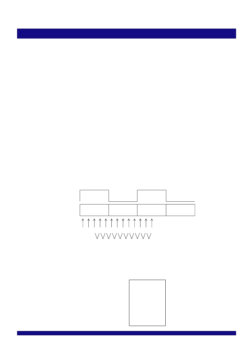
8.2.7 Software Eye-Opening Check on SPI-4
Interface
Since the SPI-4 interface is a DDR interface, both rising and falling edges
are used to update or sink data.
d
n
d
n+1
0
1
2
3
4
5
6
7
8
9
a
b
c
c
0
c
5
c
9
clock
data
over sample
position
counter
c
1
c
6
c
4
c
2
c
7
c
3
c
8
6370 drw23b
Figure 33. DDR interface and eye opening check through over sampling
Refer to the IDT88P8344 uses an internal sampling clock cycle which has
a frequency of 10 times SPI-4 clock to over-sample the data on a lane. For each
sampling clock cycle t position n data are sampled and labeled as R
t
.d
n
. The
following operation is then performed:
CNT
0
= R
t
.d
2
^ R
t
.d
3
CNT
1
= R
t
.d
3
^ R
t
.d
4
CNT
2
= R
t
.d
4
^ R
t
.d
5
CNT
3
= R
t
.d
5
^ R
t
.d
6
CNT
4
= R
t
.d
6
^ R
t
.d
7
CNT
5
= R
t
.d
7
^ R
t
.d
8
CNT
6
= R
t
.d
8
^ R
t
.d
CNT
7
= R
t
.d
^ R
t+1
.d
CNT
9
= R
t+1
.d
0
^ R
t+1
.d
1
相關PDF資料 |
PDF描述 |
|---|---|
| IDTAMB0480 | ADVANCED MEMORY BUFFER FOR FULLY BUFFERED DIMM MODULES |
| IDTCSP2510DPGI | 3.3V PHASE-LOCK LOOP CLOCK DRIVER ZERO DELAY BUFFER |
| IDTCSP2510DPG | SENSOR OPTICAL SLOTTED 1.0MM |
| IDTCSP2510D | 3.3V PHASE-LOCK LOOP CLOCK DRIVER ZERO DELAY BUFFER |
| IDTCSPT857CNL | 2.5V - 2.6V PHASE LOCKED LOOP DIFFERENTIAL 1:10 SDRAM CLOCK DRIVER |
相關代理商/技術參數(shù) |
參數(shù)描述 |
|---|---|
| IDT88P8344BHI | 功能描述:IC SPI3-SPI4 EXCHANGE 820-PBGA RoHS:否 類別:集成電路 (IC) >> 專用 IC 系列:* 產(chǎn)品培訓模塊:Lead (SnPb) Finish for COTS Obsolescence Mitigation Program 標準包裝:1 系列:- 類型:調(diào)幀器 應用:數(shù)據(jù)傳輸 安裝類型:表面貼裝 封裝/外殼:400-BBGA 供應商設備封裝:400-PBGA(27x27) 包裝:散裝 |
| IDT89H10T4BG2ZBBC | 制造商:Integrated Device Technology Inc 功能描述:IC PCI SW 10LANE 4PORT 324BGA |
| IDT89H10T4BG2ZBBC8 | 制造商:Integrated Device Technology Inc 功能描述:IC PCI SW 10LANE 4PORT 324BGA |
| IDT89H10T4BG2ZBBCG | 功能描述:IC PCI SW 10LANE 4PORT 324BGA RoHS:是 類別:集成電路 (IC) >> 專用 IC 系列:PRECISE™ 產(chǎn)品培訓模塊:Lead (SnPb) Finish for COTS Obsolescence Mitigation Program 標準包裝:1 系列:- 類型:調(diào)幀器 應用:數(shù)據(jù)傳輸 安裝類型:表面貼裝 封裝/外殼:400-BBGA 供應商設備封裝:400-PBGA(27x27) 包裝:散裝 |
| IDT89H10T4BG2ZBBCG8 | 制造商:Integrated Device Technology Inc 功能描述:IC PCI SW 10LANE 4PORT 324BGA |
發(fā)布緊急采購,3分鐘左右您將得到回復。