- 您現(xiàn)在的位置:買賣IC網 > PDF目錄67987 > MCV18ET-I/SO FLASH, 20 MHz, RISC MICROCONTROLLER, PDSO18 PDF資料下載
參數(shù)資料
| 型號: | MCV18ET-I/SO |
| 元件分類: | 微控制器/微處理器 |
| 英文描述: | FLASH, 20 MHz, RISC MICROCONTROLLER, PDSO18 |
| 封裝: | 7.50 MM, LEAD FREE, SOIC-18 |
| 文件頁數(shù): | 13/108頁 |
| 文件大小: | 1509K |
| 代理商: | MCV18ET-I/SO |
第1頁第2頁第3頁第4頁第5頁第6頁第7頁第8頁第9頁第10頁第11頁第12頁當前第13頁第14頁第15頁第16頁第17頁第18頁第19頁第20頁第21頁第22頁第23頁第24頁第25頁第26頁第27頁第28頁第29頁第30頁第31頁第32頁第33頁第34頁第35頁第36頁第37頁第38頁第39頁第40頁第41頁第42頁第43頁第44頁第45頁第46頁第47頁第48頁第49頁第50頁第51頁第52頁第53頁第54頁第55頁第56頁第57頁第58頁第59頁第60頁第61頁第62頁第63頁第64頁第65頁第66頁第67頁第68頁第69頁第70頁第71頁第72頁第73頁第74頁第75頁第76頁第77頁第78頁第79頁第80頁第81頁第82頁第83頁第84頁第85頁第86頁第87頁第88頁第89頁第90頁第91頁第92頁第93頁第94頁第95頁第96頁第97頁第98頁第99頁第100頁第101頁第102頁第103頁第104頁第105頁第106頁第107頁第108頁
MCV18E
DS41399A-page 12
2009 Microchip Technology Inc.
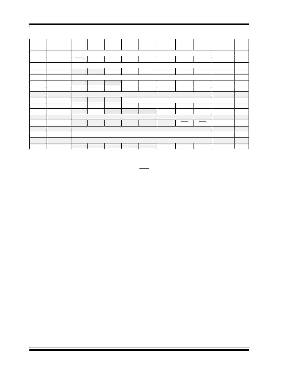
TABLE 2-2:
SPECIAL FUNCTION REGISTER SUMMARY BANK 1
Address
Name
Bit 7
Bit 6
Bit 5
Bit 4
Bit 3
Bit 2
Bit 1
Bit 0
Value on
POR, BOR
Page
80h
INDF(1)
0000 0000
81h
OPTION_REG
RBPU
INTEDG
T0CS
T0SE
PSA
PS2
PS1
PS0
1111 1111
82h
PCL(1)
Program Counter’s (PC) Least Significant Byte
0000 0000
83h
STATUS(1)
IRP(4)
RP1(4)
RP0
TO
PD
ZDC
C
0001 1xxx
84h
FSR(1)
Indirect Data Memory Address Pointer
xxxx xxxx
85h
TRISA
—
—(7)
TRISA4
TRISA3
TRISA2
TRISA1
TRISA0
---1 1111
86h
TRISB
TRISB7
TRISB6
TRISB5
TRISB4
TRISB3
TRISB2
TRISB1
TRISB0
1111 1111
87h-89h
—
Unimplemented
—
8Ah
PCLATH(1,2)
—
Write Buffer for the upper 5 bits of the Program Counter
---0 0000
8Bh
INTCON(1)
GIE
PEIE
T0IE
INTE
RBIE
T0IF
INTF
RBIF
0000 000x
8Ch
PIE1
—ADIE
—
CCP1IE
TMR2IE
TMR1IE
-0-- -000
8Dh
—
Unimplemented
—
8Eh
PCON
—
—POR
BOR
---- --qq
8Fh-91h
—
Unimplemented
—
92h
PR2
Timer2 Period Register
1111 1111
93h-9Eh
—
Unimplemented
—
9Fh
ADCON1
—
PCFG2
PCFG1
PCFG0
---- -000
Legend:
x
= unknown, u = unchanged, q = value depends on condition, - = unimplemented, read as ‘0’, Shaded locations are unimplemented,
read as ‘0’.
Note
1:
These registers can be addressed from either bank.
2:
The upper byte of the program counter is not directly accessible. PCLATH is a holding register for PC<12:8> whose contents are
transferred to the upper byte of the program counter.
3:
Other (non Power-up) Resets include: external Reset through MCLR and the Watchdog Timer Reset.
4:
The IRP and RP1 bits are reserved. Always maintain these bits clear.
5:
On any device Reset, these pins are configured as inputs.
6:
This is the value that will be in the PORT output latch.
7:
Reserved bits, do not use.
相關PDF資料 |
PDF描述 |
|---|---|
| MCV18E-I/P | 32-BIT, FLASH, 20 MHz, RISC MICROCONTROLLER, PDIP18 |
| MD8086-2/B | 16-BIT, 8 MHz, MICROPROCESSOR, CDIP40 |
| MD80C154-12/883D | 8-BIT, 12 MHz, MICROCONTROLLER, CDIP40 |
| MR83C154TXXX-20/883 | 8-BIT, MROM, 20 MHz, MICROCONTROLLER, CQCC44 |
| MR83C154XXX-20/883D | 8-BIT, MROM, 20 MHz, MICROCONTROLLER, CQCC44 |
相關代理商/技術參數(shù) |
參數(shù)描述 |
|---|---|
| MC-V190H | 制造商:Panasonic Industrial Company 功能描述:FILTER KIT |
| M-CV193H | 制造商:Panasonic Industrial Company 功能描述:OD005 |
| MC-V193H | 制造商:Panasonic Industrial Company 功能描述:FILTER KIT |
| MCV19ES | 制造商:Mencom 功能描述: |
| MCV-19FP-FW | 制造商:Mencom 功能描述: |
發(fā)布緊急采購,3分鐘左右您將得到回復。