- 您現(xiàn)在的位置:買(mǎi)賣(mài)IC網(wǎng) > PDF目錄67987 > MCV18ET-I/SO FLASH, 20 MHz, RISC MICROCONTROLLER, PDSO18 PDF資料下載
參數(shù)資料
| 型號(hào): | MCV18ET-I/SO |
| 元件分類(lèi): | 微控制器/微處理器 |
| 英文描述: | FLASH, 20 MHz, RISC MICROCONTROLLER, PDSO18 |
| 封裝: | 7.50 MM, LEAD FREE, SOIC-18 |
| 文件頁(yè)數(shù): | 87/108頁(yè) |
| 文件大小: | 1509K |
| 代理商: | MCV18ET-I/SO |
第1頁(yè)第2頁(yè)第3頁(yè)第4頁(yè)第5頁(yè)第6頁(yè)第7頁(yè)第8頁(yè)第9頁(yè)第10頁(yè)第11頁(yè)第12頁(yè)第13頁(yè)第14頁(yè)第15頁(yè)第16頁(yè)第17頁(yè)第18頁(yè)第19頁(yè)第20頁(yè)第21頁(yè)第22頁(yè)第23頁(yè)第24頁(yè)第25頁(yè)第26頁(yè)第27頁(yè)第28頁(yè)第29頁(yè)第30頁(yè)第31頁(yè)第32頁(yè)第33頁(yè)第34頁(yè)第35頁(yè)第36頁(yè)第37頁(yè)第38頁(yè)第39頁(yè)第40頁(yè)第41頁(yè)第42頁(yè)第43頁(yè)第44頁(yè)第45頁(yè)第46頁(yè)第47頁(yè)第48頁(yè)第49頁(yè)第50頁(yè)第51頁(yè)第52頁(yè)第53頁(yè)第54頁(yè)第55頁(yè)第56頁(yè)第57頁(yè)第58頁(yè)第59頁(yè)第60頁(yè)第61頁(yè)第62頁(yè)第63頁(yè)第64頁(yè)第65頁(yè)第66頁(yè)第67頁(yè)第68頁(yè)第69頁(yè)第70頁(yè)第71頁(yè)第72頁(yè)第73頁(yè)第74頁(yè)第75頁(yè)第76頁(yè)第77頁(yè)第78頁(yè)第79頁(yè)第80頁(yè)第81頁(yè)第82頁(yè)第83頁(yè)第84頁(yè)第85頁(yè)第86頁(yè)當(dāng)前第87頁(yè)第88頁(yè)第89頁(yè)第90頁(yè)第91頁(yè)第92頁(yè)第93頁(yè)第94頁(yè)第95頁(yè)第96頁(yè)第97頁(yè)第98頁(yè)第99頁(yè)第100頁(yè)第101頁(yè)第102頁(yè)第103頁(yè)第104頁(yè)第105頁(yè)第106頁(yè)第107頁(yè)第108頁(yè)
MCV18E
DS41399A-page 8
2009 Microchip Technology Inc.
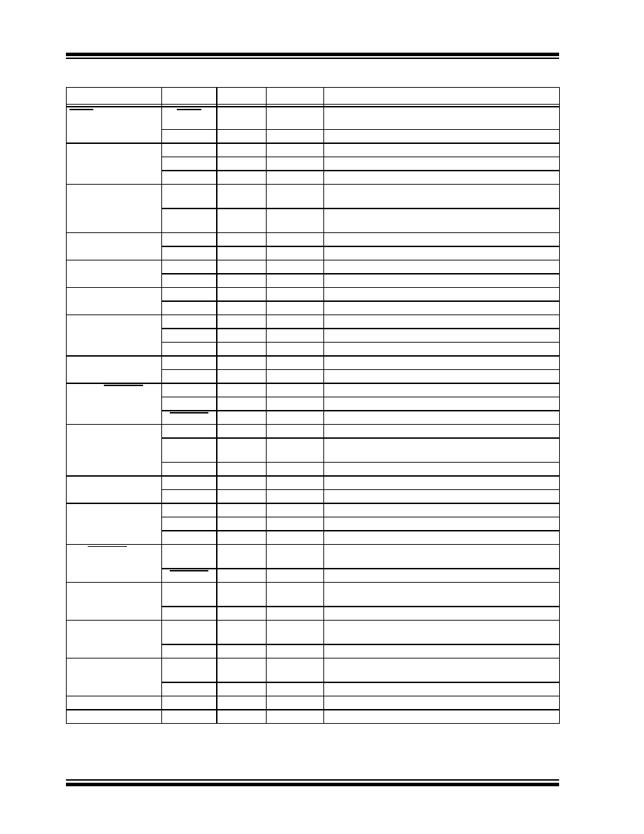
TABLE 1-1:
MCV18E PINOUT DESCRIPTION
Name
Function
Input Type
Output Type
Description
MCLR/VPP
MCLR
ST
—
Master clear (Reset) input. This pin is an active-low Reset to
the device.
VPP
P
—
Programming voltage input
OSC1/CLKIN
OSC1
XTAL
—
Oscillator crystal input
CLKIN
CMOS
—
External clock source input
CLKIN
ST
—
RC Oscillator mode
OSC2/CLKOUT
OSC2
XTAL
—
Oscillator crystal output. Connects to crystal or resonator in
Crystal Oscillator mode.
CLKOUT
—
CMOS
In RC mode, OSC2 pin outputs CLKOUT which has 1/4 the
frequency of OSC1, and denotes the instruction cycle rate.
RA0/AN0
RA0
TTL
CMOS
Bidirectional I/O
AN0
AN
—
Analog Channel 0 input
RA1/AN1
RA1
TTL
CMOS
Bidirectional I/O
AN1
AN
—
Analog Channel 1 input
RA2/AN2
RA2
TTL
CMOS
Bidirectional I/O
AN2
AN
—
Analog Channel 2 input
RA3/AN3/VREF
RA3
TTL
CMOS
Bidirectional I/O
AN3
AN
—
Analog Channel 3 input
VREF
AN
—
A/D reference voltage input
RA4/T0CKI
RA4
ST
OD
Bidirectional I/O. Open drain when configured as output.
T0CKI
ST
—
Timer0 external clock input
RB0/INT/ECCPAS2
RB0
TTL
CMOS
Bidirectional I/O. Programmable weak pull-up.
INT
ST
—
External Interrupt
ECCPAS2
ST
—
ECCP Auto-Shutdown pin
RB1/T1OSO/T1CKI
RB1
TTL
CMOS
Bidirectional I/O. Programmable weak pull-up.
T1OSO
—
XTAL
Timer1 oscillator output. Connects to crystal in Oscillator
mode.
T1CKI
ST
—
Timer1 external clock input
RB2/T1OSI
RB2
TTL
CMOS
Bidirectional I/O. Programmable weak pull-up.
T1OSI
XTAL
—
Timer1 oscillator input. Connects to crystal in Oscillator mode.
RB3/CCP1/P1A
RB3
TTL
CMOS
Bidirectional I/O. Programmable weak pull-up.
CCP1
ST
CMOS
Capture1 input, Compare1 output, PWM1 output.
P1A
—
CMOS
PWM P1A output
RB4/ECCPAS0
RB4
TTL
CMOS
Bidirectional I/O. Programmable weak pull-up. Interrupt-on-
change.
ECCPAS0
ST
—
ECCP Auto-Shutdown pin
RB5/P1B
RB5
TTL
CMOS
Bidirectional I/O. Programmable weak pull-up. Interrupt-on-
change.
P1B
—
CMOS
PWM P1B output
RB6/P1C
RB6
TTL
CMOS
Bidirectional I/O. Programmable weak pull-up. Interrupt-on-
change. ST input when used as ICSP programming clock.
P1C
—
CMOS
PWM P1C output
RB7/P1D
RB7
TTL
CMOS
Bidirectional I/O. Programmable weak pull-up. Interrupt-on-
change. ST input when used as ICSP programming data.
P1D
—
CMOS
PWM P1D output
VSS
P
—
Ground reference for logic and I/O pins.
VDD
P
—
Positive supply for logic and I/O pins.
Legend:
I
= Input
AN
= Analog input or output
OD
= Open drain
O = Output
TTL
= TTL compatible input
ST
= Schmitt Trigger input with CMOS levels
P = Power
XTAL = Crystal
CMOS = CMOS compatible input or output
相關(guān)PDF資料 |
PDF描述 |
|---|---|
| MCV18E-I/P | 32-BIT, FLASH, 20 MHz, RISC MICROCONTROLLER, PDIP18 |
| MD8086-2/B | 16-BIT, 8 MHz, MICROPROCESSOR, CDIP40 |
| MD80C154-12/883D | 8-BIT, 12 MHz, MICROCONTROLLER, CDIP40 |
| MR83C154TXXX-20/883 | 8-BIT, MROM, 20 MHz, MICROCONTROLLER, CQCC44 |
| MR83C154XXX-20/883D | 8-BIT, MROM, 20 MHz, MICROCONTROLLER, CQCC44 |
相關(guān)代理商/技術(shù)參數(shù) |
參數(shù)描述 |
|---|---|
| MC-V190H | 制造商:Panasonic Industrial Company 功能描述:FILTER KIT |
| M-CV193H | 制造商:Panasonic Industrial Company 功能描述:OD005 |
| MC-V193H | 制造商:Panasonic Industrial Company 功能描述:FILTER KIT |
| MCV19ES | 制造商:Mencom 功能描述: |
| MCV-19FP-FW | 制造商:Mencom 功能描述: |
發(fā)布緊急采購(gòu),3分鐘左右您將得到回復(fù)。