- 您現(xiàn)在的位置:買賣IC網(wǎng) > PDF目錄67987 > MCV18ET-I/SO FLASH, 20 MHz, RISC MICROCONTROLLER, PDSO18 PDF資料下載
參數(shù)資料
| 型號: | MCV18ET-I/SO |
| 元件分類: | 微控制器/微處理器 |
| 英文描述: | FLASH, 20 MHz, RISC MICROCONTROLLER, PDSO18 |
| 封裝: | 7.50 MM, LEAD FREE, SOIC-18 |
| 文件頁數(shù): | 85/108頁 |
| 文件大小: | 1509K |
| 代理商: | MCV18ET-I/SO |
第1頁第2頁第3頁第4頁第5頁第6頁第7頁第8頁第9頁第10頁第11頁第12頁第13頁第14頁第15頁第16頁第17頁第18頁第19頁第20頁第21頁第22頁第23頁第24頁第25頁第26頁第27頁第28頁第29頁第30頁第31頁第32頁第33頁第34頁第35頁第36頁第37頁第38頁第39頁第40頁第41頁第42頁第43頁第44頁第45頁第46頁第47頁第48頁第49頁第50頁第51頁第52頁第53頁第54頁第55頁第56頁第57頁第58頁第59頁第60頁第61頁第62頁第63頁第64頁第65頁第66頁第67頁第68頁第69頁第70頁第71頁第72頁第73頁第74頁第75頁第76頁第77頁第78頁第79頁第80頁第81頁第82頁第83頁第84頁當(dāng)前第85頁第86頁第87頁第88頁第89頁第90頁第91頁第92頁第93頁第94頁第95頁第96頁第97頁第98頁第99頁第100頁第101頁第102頁第103頁第104頁第105頁第106頁第107頁第108頁
MCV18E
DS41399A-page 78
2009 Microchip Technology Inc.
9.12
Watchdog Timer (WDT)
The Watchdog Timer is a free running, on-chip, RC
oscillator
which
does
not
require
any
external
components. This RC oscillator is separate from the RC
oscillator of the OSC1/CLKIN pin. That means that the
WDT will run, even if the clock on the OSC1/CLKIN and
OSC2/CLKOUT pins of the device have been stopped,
for example, by execution of a SLEEP instruction.
During normal operation, a WDT time-out generates a
device Reset (Watchdog Timer Reset). If the device is in
Sleep mode, a WDT time-out causes the device to
wake-up and continue with normal operation (Watchdog
Timer Wake-up). The TO bit in the STATUS register will
be cleared upon a Watchdog Timer time-out.
The WDT can be permanently disabled by clearing
Configuration bit WDTE (Section 9.1 “Configuration
WDT time-out period values may be found in the
Electrical Specifications section under TWDT (parameter
#31). Values for the WDT prescaler (actually a
postscaler, but shared with the Timer0 prescaler) may
be assigned using the OPTION register.
.
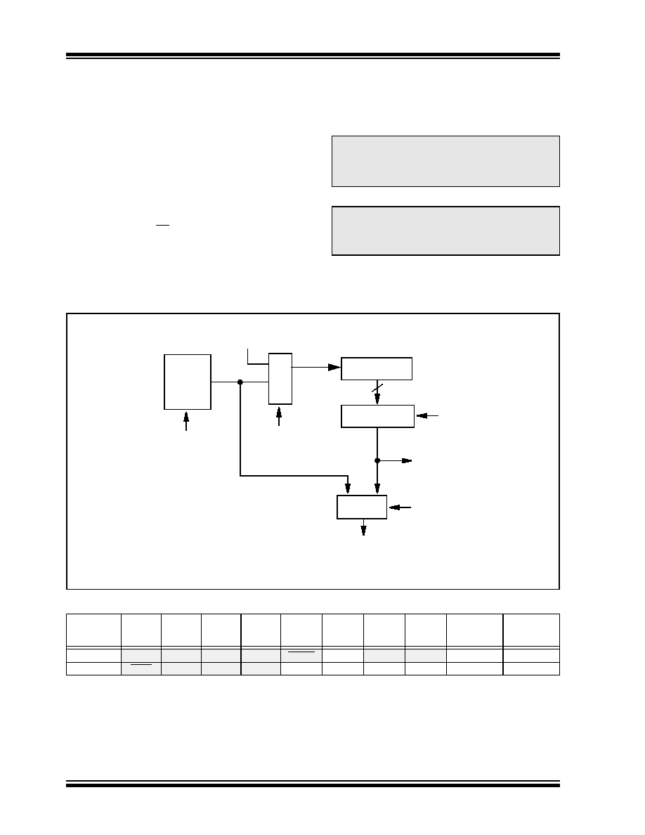
FIGURE 9-14:
WATCHDOG TIMER BLOCK DIAGRAM
TABLE 9-7:
SUMMARY OF REGISTERS ASSOCIATED WITH WATCHDOG TIMER
Note:
The CLRWDT and SLEEP instructions clear
the WDT and the postscaler, if assigned to
the WDT, and prevent it from timing out
and generating a device Reset condition.
Note:
When a CLRWDT instruction is executed
and the prescaler is assigned to the WDT,
the prescaler count will be cleared, but the
prescaler assignment is not changed.
Name
Bit 7
Bit 6
Bit 5
Bit 4
Bit 3
Bit 2
Bit 1
Bit 0
Value on
POR, BOR
Value on
all other
Resets
CONFIG1(1)
BORV
BOREN
—
PWRTE
WDTE
FOSC1
FOSC0
—
OPTION_REG
RBPU
INTEDG
T0CS
T0SE
PSA
PS2
PS1
PS0
1111 1111
Legend:
x
= unknown, u = unchanged, - = unimplemented locations read as ‘0’. Shaded cells are not used the Watchdog Timer.
Note
1:
See Configuration Word Register (Register 9-1) for operation of all register bits.
From TMR0 Clock Source (Figure 4-1)
To TMR0 (Figure 4-1)
Postscaler
WDT Timer
WDT
Enable Bit
0
1
M
U
X
PSA
8-to-1 MUX
PS2:PS0
0
1
MUX
PSA
WDT
Time-out
8
Note:
PSA and PS2:PS0 are bits in the OPTION register.
相關(guān)PDF資料 |
PDF描述 |
|---|---|
| MCV18E-I/P | 32-BIT, FLASH, 20 MHz, RISC MICROCONTROLLER, PDIP18 |
| MD8086-2/B | 16-BIT, 8 MHz, MICROPROCESSOR, CDIP40 |
| MD80C154-12/883D | 8-BIT, 12 MHz, MICROCONTROLLER, CDIP40 |
| MR83C154TXXX-20/883 | 8-BIT, MROM, 20 MHz, MICROCONTROLLER, CQCC44 |
| MR83C154XXX-20/883D | 8-BIT, MROM, 20 MHz, MICROCONTROLLER, CQCC44 |
相關(guān)代理商/技術(shù)參數(shù) |
參數(shù)描述 |
|---|---|
| MC-V190H | 制造商:Panasonic Industrial Company 功能描述:FILTER KIT |
| M-CV193H | 制造商:Panasonic Industrial Company 功能描述:OD005 |
| MC-V193H | 制造商:Panasonic Industrial Company 功能描述:FILTER KIT |
| MCV19ES | 制造商:Mencom 功能描述: |
| MCV-19FP-FW | 制造商:Mencom 功能描述: |
發(fā)布緊急采購,3分鐘左右您將得到回復(fù)。