- 您現(xiàn)在的位置:買賣IC網(wǎng) > PDF目錄67987 > MCV18ET-I/SO FLASH, 20 MHz, RISC MICROCONTROLLER, PDSO18 PDF資料下載
參數(shù)資料
| 型號: | MCV18ET-I/SO |
| 元件分類: | 微控制器/微處理器 |
| 英文描述: | FLASH, 20 MHz, RISC MICROCONTROLLER, PDSO18 |
| 封裝: | 7.50 MM, LEAD FREE, SOIC-18 |
| 文件頁數(shù): | 92/108頁 |
| 文件大?。?/td> | 1509K |
| 代理商: | MCV18ET-I/SO |
第1頁第2頁第3頁第4頁第5頁第6頁第7頁第8頁第9頁第10頁第11頁第12頁第13頁第14頁第15頁第16頁第17頁第18頁第19頁第20頁第21頁第22頁第23頁第24頁第25頁第26頁第27頁第28頁第29頁第30頁第31頁第32頁第33頁第34頁第35頁第36頁第37頁第38頁第39頁第40頁第41頁第42頁第43頁第44頁第45頁第46頁第47頁第48頁第49頁第50頁第51頁第52頁第53頁第54頁第55頁第56頁第57頁第58頁第59頁第60頁第61頁第62頁第63頁第64頁第65頁第66頁第67頁第68頁第69頁第70頁第71頁第72頁第73頁第74頁第75頁第76頁第77頁第78頁第79頁第80頁第81頁第82頁第83頁第84頁第85頁第86頁第87頁第88頁第89頁第90頁第91頁當前第92頁第93頁第94頁第95頁第96頁第97頁第98頁第99頁第100頁第101頁第102頁第103頁第104頁第105頁第106頁第107頁第108頁
MCV18E
DS41399A-page 84
2009 Microchip Technology Inc.
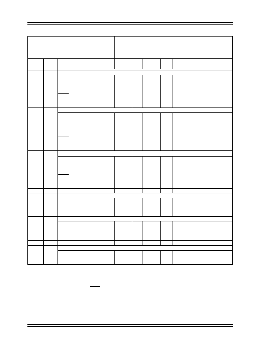
10.3
DC Characteristics: MCV18E (Industrial)
DC CHARACTERISTICS
Standard Operating Conditions (unless otherwise stated)
Operating temperature
-40°C
≤ TA ≤ +85°C for industrial
Param
No.
Sym
Characteristic
Min
Typ
Max
Units
Conditions
Input Low Voltage
VIL
I/O ports
D030
D030A
with TTL buffer
VSS
—
0.8
0.15 VDD
V
4.5V
≤ VDD ≤ 5.5V
otherwise
D031
with Schmitt Trigger buffer
VSS
—0.2 VDD
V
D032
MCLR, OSC1 (in RC mode)
VSS
—0.2 VDD
V
D033
OSC1 (in HS mode)
OSC1 (in XT and LP modes)
VSS
—
0.3 VDD
0.6
V
(Note1)
Input High Voltage
VIH
I/O ports
—
D040
with TTL buffer
2.4
—
VDD
V4.5V
≤ VDD ≤ 5.5V
D040A
0.25 VDD
+ 0.8V
—VDD
V
otherwise
D041
with Schmitt Trigger buffer
0.8 VDD
—VDD
V
For entire VDD range
D042
MCLR
0.8 VDD
—VDD
V
D042A
OSC1 (XT, HS and LP modes)
0.7 VDD
—VDD
V
(Note1)
D043
OSC1 (in RC mode)
0.9 VDD
—VDD
V
Input Leakage Current(2), (3)
D060
IIL
I/O ports
—
±1
±500
μA
nA
Vss
≤ VPIN ≤ VDD, Pin at
high-impedance
Vss
≤ VPIN ≤ VDD, Pin configured as
analog input
D061
MCLR, RA4/T0CKI
—
±5
μA
Vss
≤ VPIN ≤ VDD
D063
OSC1/CLKIN
—
±5
μA
Vss
≤ VPIN ≤ VDD, XT, HS and LP Osc
modes
D070
IPURB
PORTB weak pull-up current
50
250
400
μAVDD = 5V, VPIN = VSS
Output Low Voltage
D080
VOL
I/O ports
—
0.6
V
IOL = 8.5 mA, VDD = 4.5V, -40
°C to
+85
°C
D083
OSC2/CLKOUT (RC Osc mode)
—
0.6
V
IOL = 1.6 mA, VDD = 4.5V, -40
°C to
+85
°C
Output High Voltage
D090
VOH
I/O ports(3)
VDD-0.7
—
V
IOH = -3.0 mA, VDD = 4.5V, -40
°C to
+85
°C
D092
OSC2/CLKOUT (RC Osc mode)
VDD-0.7
—
V
IOH = -1.3 mA, VDD = 4.5V, -40
°C to
+85
°C
D150*
VOD
Open-Drain High Voltage
—
8.5
V
RA4 pin
Capacitive Loading Specs on Output Pins
D100
COSC2 OSC2/CLKOUT pin
—
15
pF
In XT, HS and LP modes when exter-
nal clock is used to drive OSC1.
D101
CIO
All I/O pins and OSC2 (in RC mode)
—
50
pF
*
These parameters are characterized but not tested.
Data in “Typ” column is at 5V, 25
°C unless otherwise stated. These parameters are for design guidance only and are not
tested.
Note
1:
In RC Oscillator mode, the OSC1/CLKIN pin is a Schmitt Trigger input. It is not recommended that the PIC device be
driven with external clock in RC mode.
2:
The leakage current on the MCLR/VPP pin is strongly dependent on the applied voltage level. The specified levels repre-
sent normal operating conditions. Higher leakage current may be measured at different input voltages.
3:
Negative current is defined as current sourced by the pin.
相關(guān)PDF資料 |
PDF描述 |
|---|---|
| MCV18E-I/P | 32-BIT, FLASH, 20 MHz, RISC MICROCONTROLLER, PDIP18 |
| MD8086-2/B | 16-BIT, 8 MHz, MICROPROCESSOR, CDIP40 |
| MD80C154-12/883D | 8-BIT, 12 MHz, MICROCONTROLLER, CDIP40 |
| MR83C154TXXX-20/883 | 8-BIT, MROM, 20 MHz, MICROCONTROLLER, CQCC44 |
| MR83C154XXX-20/883D | 8-BIT, MROM, 20 MHz, MICROCONTROLLER, CQCC44 |
相關(guān)代理商/技術(shù)參數(shù) |
參數(shù)描述 |
|---|---|
| MC-V190H | 制造商:Panasonic Industrial Company 功能描述:FILTER KIT |
| M-CV193H | 制造商:Panasonic Industrial Company 功能描述:OD005 |
| MC-V193H | 制造商:Panasonic Industrial Company 功能描述:FILTER KIT |
| MCV19ES | 制造商:Mencom 功能描述: |
| MCV-19FP-FW | 制造商:Mencom 功能描述: |
發(fā)布緊急采購,3分鐘左右您將得到回復(fù)。