- 您現(xiàn)在的位置:買(mǎi)賣(mài)IC網(wǎng) > PDF目錄358635 > 38D5 (Renesas Technology Corp.) SINGLE-CHIP 8-BIT CMOS MICROCOMPUTER PDF資料下載
參數(shù)資料
| 型號(hào): | 38D5 |
| 廠商: | Renesas Technology Corp. |
| 英文描述: | SINGLE-CHIP 8-BIT CMOS MICROCOMPUTER |
| 中文描述: | 單芯片8位CMOS微機(jī) |
| 文件頁(yè)數(shù): | 19/141頁(yè) |
| 文件大小: | 2027K |
| 代理商: | 38D5 |
第1頁(yè)第2頁(yè)第3頁(yè)第4頁(yè)第5頁(yè)第6頁(yè)第7頁(yè)第8頁(yè)第9頁(yè)第10頁(yè)第11頁(yè)第12頁(yè)第13頁(yè)第14頁(yè)第15頁(yè)第16頁(yè)第17頁(yè)第18頁(yè)當(dāng)前第19頁(yè)第20頁(yè)第21頁(yè)第22頁(yè)第23頁(yè)第24頁(yè)第25頁(yè)第26頁(yè)第27頁(yè)第28頁(yè)第29頁(yè)第30頁(yè)第31頁(yè)第32頁(yè)第33頁(yè)第34頁(yè)第35頁(yè)第36頁(yè)第37頁(yè)第38頁(yè)第39頁(yè)第40頁(yè)第41頁(yè)第42頁(yè)第43頁(yè)第44頁(yè)第45頁(yè)第46頁(yè)第47頁(yè)第48頁(yè)第49頁(yè)第50頁(yè)第51頁(yè)第52頁(yè)第53頁(yè)第54頁(yè)第55頁(yè)第56頁(yè)第57頁(yè)第58頁(yè)第59頁(yè)第60頁(yè)第61頁(yè)第62頁(yè)第63頁(yè)第64頁(yè)第65頁(yè)第66頁(yè)第67頁(yè)第68頁(yè)第69頁(yè)第70頁(yè)第71頁(yè)第72頁(yè)第73頁(yè)第74頁(yè)第75頁(yè)第76頁(yè)第77頁(yè)第78頁(yè)第79頁(yè)第80頁(yè)第81頁(yè)第82頁(yè)第83頁(yè)第84頁(yè)第85頁(yè)第86頁(yè)第87頁(yè)第88頁(yè)第89頁(yè)第90頁(yè)第91頁(yè)第92頁(yè)第93頁(yè)第94頁(yè)第95頁(yè)第96頁(yè)第97頁(yè)第98頁(yè)第99頁(yè)第100頁(yè)第101頁(yè)第102頁(yè)第103頁(yè)第104頁(yè)第105頁(yè)第106頁(yè)第107頁(yè)第108頁(yè)第109頁(yè)第110頁(yè)第111頁(yè)第112頁(yè)第113頁(yè)第114頁(yè)第115頁(yè)第116頁(yè)第117頁(yè)第118頁(yè)第119頁(yè)第120頁(yè)第121頁(yè)第122頁(yè)第123頁(yè)第124頁(yè)第125頁(yè)第126頁(yè)第127頁(yè)第128頁(yè)第129頁(yè)第130頁(yè)第131頁(yè)第132頁(yè)第133頁(yè)第134頁(yè)第135頁(yè)第136頁(yè)第137頁(yè)第138頁(yè)第139頁(yè)第140頁(yè)第141頁(yè)
Rev.3.01
REJ03B0158-0301
Aug 08, 2007
Page 19 of 134
38D5 Group
I/O PORTS
Direction Registers (Ports P0-P6, P7
2
-P7
4
)
The I/O ports P0-P6, P7
2
-P7
4
have direction registers which
determine the input/output direction of each individual pin. Each
bit in a direction register corresponds to one pin, each pin can be
set to be input port or output port.
When “0” is written to the bit of the direction register, the
corresponding pin becomes an input pin. As for ports P0
P3,
when “1” is written to the bit of the direction register and the
segment output disable register, the corresponding pin becomes
an output pin. As for ports P4
P6, P7
2
-P7
4
when “1” is written to
the bit of the direction register, the corresponding pin becomes an
output pin.
If data is read from a pin set to output, the value of the port latch
is read, not the value of the pin itself. However, when peripheral
output (RTP
1
, RTP
0
, T
XOUT1
, T
XOUT2
, T
4OUT
, T
3OUT
and
T
2OUT
/CKOUT) is selected, the output value is read. Depending
on the pin, output from a peripheral function may be read. Pins
set to input are floating. If a pin set to input is written to, only the
port output latch is written to and the pin remains floating.
Ports P7
0
, P7
1
These are input ports which are shared with the voltage
multiplier. When these are read out at using the voltage
multiplier, the contents are “1”.
Pull-up Control
Each individual bit of ports P0
P3 can be pulled up with a
program by setting direction registers and segment output disable
registers 0 to 2 (addresses 0FF4
16
to 0FF6
16
).
The pin is pulled up by setting “0” to the direction register and
“1” to the segment output disable register.
By setting the PULL registers (addresses 0FF0
16
to OFF2
16
),
ports P4
P7 can control pull-up with a program.
However, the contents of PULL register do not affect ports
programmed as the output ports.
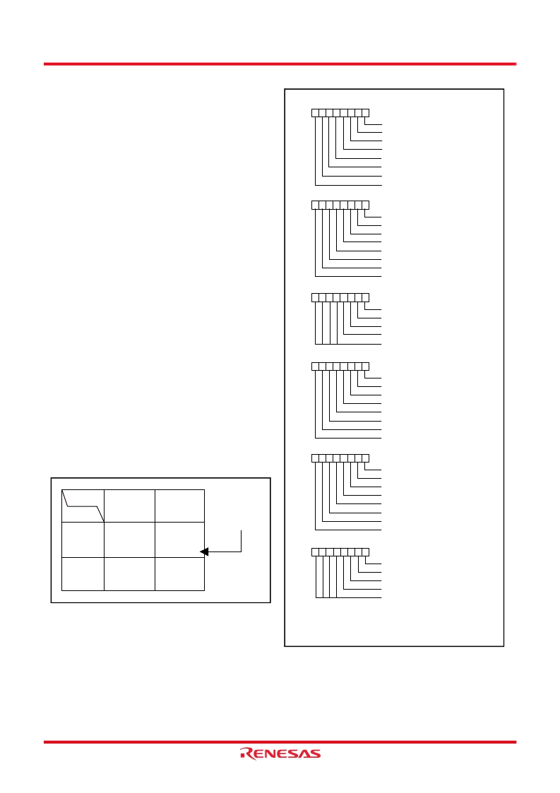
Fig. 12 Structure of ports P0 to P3
Fig. 13 Structure of PULL register and segment output
disable register
Segment output
disable register
Direction
register
Input port
No pull-up
Input port
Pull-up
Segment
output
Port output
“0”
“0”
“1”
“1”
Initial state
Note1
: The PULL register and segment output disable register affect only ports
programmed as the input ports.
P6
0
pull-up
P6
1
pull-up
P6
2
pull-up
P6
3
pull-up
P6
4
pull-up
P6
5
pull-up
P6
6
pull-up
P6
7
pull-up
PULL register 2
(PULL2 : address 0FF1
16
))
b7
b0
PULL register 1
(PULL1 : address 0FF0
16
)
b7
b0
P5
0
pull-up
P5
1
pull-up
P5
2
pull-up
P5
3
pull-up
P5
4
pull-up
P5
5
pull-up
P5
6
pull-up
P5
7
pull-up
P4
0-
P4
3
pull-up
P4
4-
P4
7
pull-up
P7
2-
P7
4
pull-up
Not used (do not write “1”)
Not used (return “0” when read)
PULL register 3
(PULL3 : address 0FF2
16
))
b7
b0
P0
0
pull-up
P0
1
pull-up
P0
2
pull-up
P0
3
pull-up
P0
4
pull-up
P0
5
pull-up
P0
6
pull-up
P0
7
pull-up
Segment output disable register 0
(SEG0 : address 0FF4
16
)
b7
b0
0 : No pull-up
1 : Pull-up
0 : No pull-up
1 : Pull-up
0 : No pull-up
1 : Pull-up
0 : No pull-up
1 : Pull-up
P2
0
pull-up
P2
1
pull-up
P2
2
pull-up
P2
3
pull-up
P2
4
pull-up
P2
5
pull-up
P2
6
pull-up
P2
7
pull-up
Segment output disable register 1
(SEG1 : address 0FF5
16
)
b7
b0
0 : No pull-up
1 : Pull-up
P1
0-
P1
3
pull-up
P1
4-
P1
7
pull-up
P3
0-
P3
3
pull-up
P3
4-
P3
7
pull-up
Not used (do not write “1”)
Segment output disable register 2
(SEG2 : address 0FF6
16
)
b7
b0
0 : No pull-up
1 : Pull-up
相關(guān)PDF資料 |
PDF描述 |
|---|---|
| 38F1222 | 300mA LDO Linear Regulators with Internal Microprocessor Reset Circuit |
| TA5M | STECKER DIN MINI 5POL |
| 70B5031 | KUPPLUNG DIN MINI 5POL |
| 39-26-3050 | 300mA LDO Linear Regulators with Internal Microprocessor Reset Circuit |
| 390KD05JX | 11 to 460 Volts Varistor 0.7 to 29 Joule |
相關(guān)代理商/技術(shù)參數(shù) |
參數(shù)描述 |
|---|---|
| 38D5_07 | 制造商:RENESAS 制造商全稱:Renesas Technology Corp 功能描述:Standard Characteristics Example |
| 38D5_08 | 制造商:RENESAS 制造商全稱:Renesas Technology Corp 功能描述:SINGLE-CHIP 8-BIT CMOS MICROCOMPUTER |
| 38D511G015FE6AD | 制造商:Sprague/Vishay 功能描述:AL015X751 |
| 38D5-FMV | 制造商:RENESAS 制造商全稱:Renesas Technology Corp 功能描述:Standard Characteristics (Flash Memory Version) |
| 38DDP11B11M1QT | 功能描述:SWITCH PUSH DPDT,O-N-O,N,SL,LF , 制造商:grayhill inc. 系列:* 零件狀態(tài):在售 標(biāo)準(zhǔn)包裝:1 |
發(fā)布緊急采購(gòu),3分鐘左右您將得到回復(fù)。