- 您現(xiàn)在的位置:買賣IC網(wǎng) > PDF目錄358635 > 38D5 (Renesas Technology Corp.) SINGLE-CHIP 8-BIT CMOS MICROCOMPUTER PDF資料下載
參數(shù)資料
| 型號(hào): | 38D5 |
| 廠商: | Renesas Technology Corp. |
| 英文描述: | SINGLE-CHIP 8-BIT CMOS MICROCOMPUTER |
| 中文描述: | 單芯片8位CMOS微機(jī) |
| 文件頁數(shù): | 36/141頁 |
| 文件大小: | 2027K |
| 代理商: | 38D5 |
第1頁第2頁第3頁第4頁第5頁第6頁第7頁第8頁第9頁第10頁第11頁第12頁第13頁第14頁第15頁第16頁第17頁第18頁第19頁第20頁第21頁第22頁第23頁第24頁第25頁第26頁第27頁第28頁第29頁第30頁第31頁第32頁第33頁第34頁第35頁當(dāng)前第36頁第37頁第38頁第39頁第40頁第41頁第42頁第43頁第44頁第45頁第46頁第47頁第48頁第49頁第50頁第51頁第52頁第53頁第54頁第55頁第56頁第57頁第58頁第59頁第60頁第61頁第62頁第63頁第64頁第65頁第66頁第67頁第68頁第69頁第70頁第71頁第72頁第73頁第74頁第75頁第76頁第77頁第78頁第79頁第80頁第81頁第82頁第83頁第84頁第85頁第86頁第87頁第88頁第89頁第90頁第91頁第92頁第93頁第94頁第95頁第96頁第97頁第98頁第99頁第100頁第101頁第102頁第103頁第104頁第105頁第106頁第107頁第108頁第109頁第110頁第111頁第112頁第113頁第114頁第115頁第116頁第117頁第118頁第119頁第120頁第121頁第122頁第123頁第124頁第125頁第126頁第127頁第128頁第129頁第130頁第131頁第132頁第133頁第134頁第135頁第136頁第137頁第138頁第139頁第140頁第141頁
Rev.3.01
REJ03B0158-0301
Aug 08, 2007
Page 36 of 134
38D5 Group
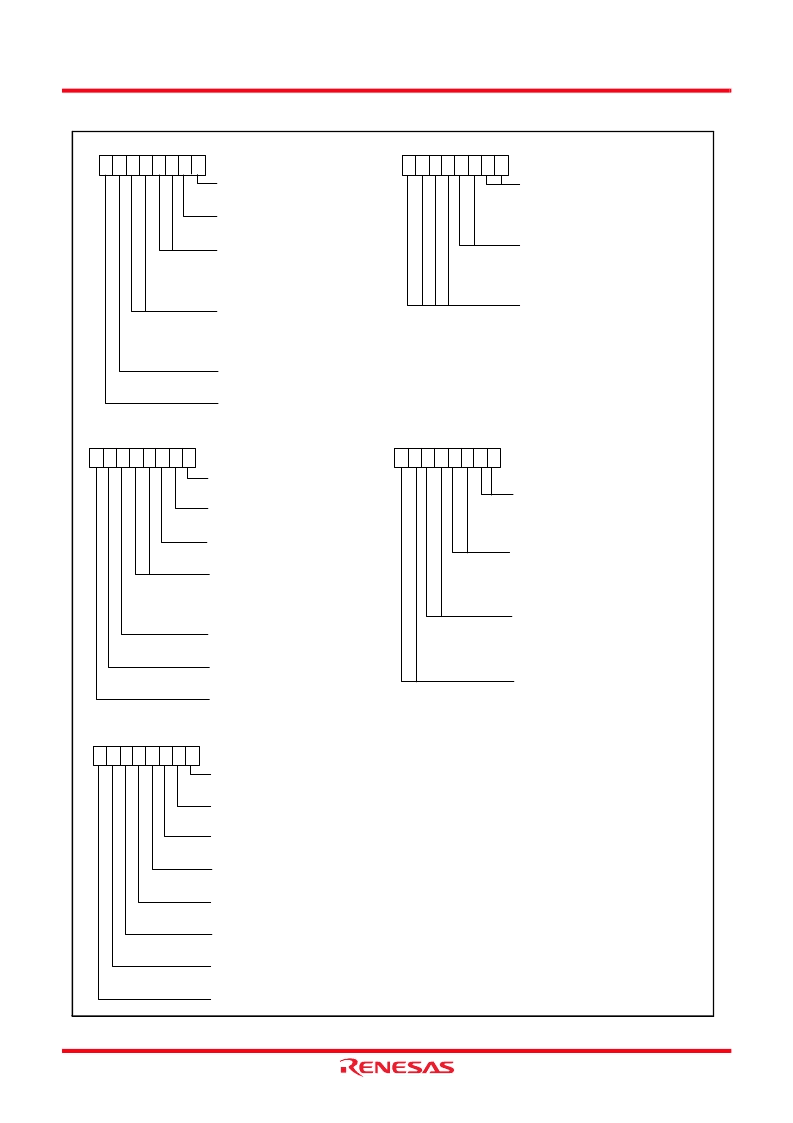
Fig. 27 Structure of Timer 1 to timer 4 related registers
Timer 12 mode register
(T12M: address 0025
16
)
Timer 34 mode register
(T34M: address 0026
16
)
Timer 3 count stop bit
0 : Count operation
1 : Count stop
Timer 4 count stop bit
0 : Count operation
1 : Count stop
Timer 1234 mode register
(T1234M: address 0027
16
)
T
3OUT
output edge switch bit
0 : Start at “L” output
1 : Start at “H” output
T
4OUT
output edge switch bit
0 : Start at “L” output
1 : Start at “H” output
Timer 1234 frequency division selection register
(PRE1234: address 0028
16
)
PWM01 register
(PWM01: address 0024
16
)
Timer 1 frequency division selection bits
b1b0
0 0 : 1/16
×
φ
SOURCE
0 1 : 1/1
×
φ
SOURCE
1 0 : 1/2
×
φ
SOURCE
1 1 : 1/256
×
φ
SOURCE
Timer 2 frequency division selection bits
b3b2
0 0 : 1/16
×
φ
SOURCE
0 1 : 1/1
×
φ
SOURCE
1 0 : 1/2
×
φ
SOURCE
1 1 : 1/256
×
φ
SOURCE
Timer 3 frequency division selection bits
b5b4
0 0 : 1/16
×
φ
SOURCE
0 1 : 1/1
×
φ
SOURCE
1 0 : 1/2
×
φ
SOURCE
1 1 : 1/256
×
φ
SOURCE
Timer 1 count stop bit
0 : Count operation
1 : Count stop
T
2OUT
output edge switch bit
0 : Start at “L” output
1 : Start at “H” output
Timer 2 output selection bit (P7
2
)
0 : I/O port
1 : Timer 2 output
Timer 2 count source selection bits
b5b4
0 0 : Underflow of Timer 1
0 1 : f(X
CIN
)
1 0 : Frequency divider for Timer 2
1 1 : Not available
Timer 1 count source selection bits
b3b2
0 0 : Frequency divider for Timer 1
0 1 : f(X
CIN
)
1 0 : Underflow of Timer Y
1 1 : Not available
Timer 2 count stop bit
0 : Count operation
1 : Count stop
PWM0 set bits
b1b0
0 0 : No extended
0 1 : Extended once in four periods
1 0 : Extended twice in four periods
1 1 : Extended three times in four periods
PWM1 set bits
b3b2
0 0 : No extended
0 1 : Extended once in four periods
1 0 : Extended twice in four periods
1 1 : Extended three times in four periods
Not used (returns “0” when read)
Timer 4 frequency division selection bits
b7b6
0 0 : 1/16
×
φ
SOURCE
0 1 : 1/1
×
φ
SOURCE
1 0 : 1/2
×
φ
SOURCE
1 1 : 1/256
×
φ
SOURCE
Not used (returns “0” when read)
Timer 4 write control bit
0 : Write data to both timer latch and timer
1 : Write data to timer latch only
Timer 3 write control bit
0 : Write data to both timer latch and timer
1 : Write data to timer latch only
Timer 2 write control bit
0 : Write data to both timer latch and timer
1 : Write data to timer latch only
Timer 4 output selection bit (P7
4
)
0 : I/O port
1 : Timer 4 output
Timer 3 output selection bit (P7
3
)
0 : I/O port
1 : Timer 3 output
Not used (returns “0” when read)
Timer 4 operating mode selection bit
0 : Timer mode
1 : PWM mode
Timer 3 operating mode selection bit
0 : Timer mode
1 : PWM mode
Timer 4 count source selection bits
b4b3
0 0 : Frequency divider for Timer 4
0 1 : Underflow of Timer 3
1 0 : Underflow of Timer 2
1 1 : f(X
IN
)
Timer 3 count source selection bit
0 : Frequency divider for Timer 3
1 : Underflow of Timer 2
b7
b0
b7
b0
b7
b0
b7
b0
b7
b0
Note1:
φ
SOURCE indicates the followings:
X
IN
input in the frequency/2, 4, or 8 mode
On-chip oscillator divided by 4 in the on-chip oscillator mode
Sub-clock in the low-speed mode
(1)
相關(guān)PDF資料 |
PDF描述 |
|---|---|
| 38F1222 | 300mA LDO Linear Regulators with Internal Microprocessor Reset Circuit |
| TA5M | STECKER DIN MINI 5POL |
| 70B5031 | KUPPLUNG DIN MINI 5POL |
| 39-26-3050 | 300mA LDO Linear Regulators with Internal Microprocessor Reset Circuit |
| 390KD05JX | 11 to 460 Volts Varistor 0.7 to 29 Joule |
相關(guān)代理商/技術(shù)參數(shù) |
參數(shù)描述 |
|---|---|
| 38D5_07 | 制造商:RENESAS 制造商全稱:Renesas Technology Corp 功能描述:Standard Characteristics Example |
| 38D5_08 | 制造商:RENESAS 制造商全稱:Renesas Technology Corp 功能描述:SINGLE-CHIP 8-BIT CMOS MICROCOMPUTER |
| 38D511G015FE6AD | 制造商:Sprague/Vishay 功能描述:AL015X751 |
| 38D5-FMV | 制造商:RENESAS 制造商全稱:Renesas Technology Corp 功能描述:Standard Characteristics (Flash Memory Version) |
| 38DDP11B11M1QT | 功能描述:SWITCH PUSH DPDT,O-N-O,N,SL,LF , 制造商:grayhill inc. 系列:* 零件狀態(tài):在售 標(biāo)準(zhǔn)包裝:1 |
發(fā)布緊急采購,3分鐘左右您將得到回復(fù)。