- 您現(xiàn)在的位置:買賣IC網(wǎng) > PDF目錄378210 > 80546KF (Intel Corp.) 64-bit Intel Xeon Processor MP with up to 8MB L3 Cache PDF資料下載
參數(shù)資料
| 型號: | 80546KF |
| 廠商: | Intel Corp. |
| 英文描述: | 64-bit Intel Xeon Processor MP with up to 8MB L3 Cache |
| 中文描述: | 64位Intel Xeon處理器MP的高達8MB三級高速緩存 |
| 文件頁數(shù): | 25/138頁 |
| 文件大小: | 2666K |
| 代理商: | 80546KF |
第1頁第2頁第3頁第4頁第5頁第6頁第7頁第8頁第9頁第10頁第11頁第12頁第13頁第14頁第15頁第16頁第17頁第18頁第19頁第20頁第21頁第22頁第23頁第24頁當前第25頁第26頁第27頁第28頁第29頁第30頁第31頁第32頁第33頁第34頁第35頁第36頁第37頁第38頁第39頁第40頁第41頁第42頁第43頁第44頁第45頁第46頁第47頁第48頁第49頁第50頁第51頁第52頁第53頁第54頁第55頁第56頁第57頁第58頁第59頁第60頁第61頁第62頁第63頁第64頁第65頁第66頁第67頁第68頁第69頁第70頁第71頁第72頁第73頁第74頁第75頁第76頁第77頁第78頁第79頁第80頁第81頁第82頁第83頁第84頁第85頁第86頁第87頁第88頁第89頁第90頁第91頁第92頁第93頁第94頁第95頁第96頁第97頁第98頁第99頁第100頁第101頁第102頁第103頁第104頁第105頁第106頁第107頁第108頁第109頁第110頁第111頁第112頁第113頁第114頁第115頁第116頁第117頁第118頁第119頁第120頁第121頁第122頁第123頁第124頁第125頁第126頁第127頁第128頁第129頁第130頁第131頁第132頁第133頁第134頁第135頁第136頁第137頁第138頁
64-bit Intel
Xeon Processor MP with up to 8MB L3 Cache Datasheet
25
Electrical Specifications
2.6
Front Side Bus Signal Groups
The front side bus signals are grouped by buffer type as listed in
Table 2-5
. The buffer type
indicates which AC and DC specifications apply to the signals. AGTL+ input signals have
differential input buffers that use GTLREF as a reference level. In this document, the term “AGTL+
Input” refers to the AGTL+ input group as well as the AGTL+ I/O group when receiving. Similarly,
“AGTL+ Output” refers to the AGTL+ output group as well as the AGTL+ I/O group when driving.
AGTL+ asynchronous outputs can become active anytime and include an active pMOS pull-up
transistor to assist during the first clock of a low-to-high voltage transition.
Implementing a source synchronous data bus requires specifying two sets of timing parameters.
One set is for common clock signals which are dependent upon the rising edge of BCLK0 (ADS#,
HIT#, HITM#, etc.). The second set is for the source synchronous signals that are relative to their
respective strobe lines (data and address) as well as the rising edge of BCLK0. Asynchronous
signals are present (A20M#, IGNNE#, etc.) and can become active at any time during the clock
cycle.
Table 2-5
identifies signals as common clock, source synchronous, and asynchronous.
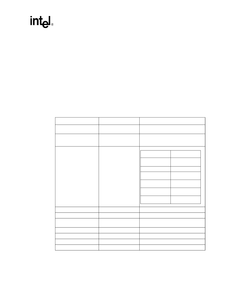
Table 2-5. Front Side Bus Pin Groups (Sheet 1 of 2)
Signal Group
Type
Signals
1
AGTL+ Common Clock Input
Synchronous to BCLK[1:0]
BPRI#, BR[3:1]#, DEFER#, ID[7:0]#, IDS#,
OOD#, RESET#, RS[2:0]#, RSP#, TRDY#
AGTL+ Common Clock I/O
Synchronous to BCLK[1:0]
ADS#, AP[1:0]#, BINIT#, BNR#, BPM[5:0]#,
BR0#, DBSY#, DP[3:0]#, DRDY#, HIT#,
HITM#, LOCK#, MCERR#
AGTL+ Source Synchronous
I/O
Synchronous to associated
strobe
AGTL+ Strobe Input/Output
Synchronous to BCLK[1:0]
ADSTB[1:0]#, DSTBP[3:0]#, DSTBN[3:0]#
AGTL+ Asynchronous Output
Asynchronous
FERR#/PBE#, IERR#, PROCHOT#
GTL+ Asynchronous Input
Asynchronous
A20M#, FORCEPR#, IGNNE#, INIT#, LINT0/
INTR, LINT1/NMI, SMI#, STPCLK#
GTL+ Asynchronous Output
Asynchronous
THERMTRIP#
TAP Input
Synchronous to TCK
TCK, TDI, TMS
TAP Input
Asynchronous
TRST#
TAP Output
Synchronous to TCK
TDO
Signals
Associated Strobe
REQ[4:0]#,
A[37:36,16:3]#
ADSTB0#
A[39:38,35:17]#
ADSTB1#
D[15:0]#, DEP[1:0]#,
DBI0#
DSTBP0#, DSTBN0#
D[31:16]#, DEP[3:2]#,
DBI1#
DSTBP1#, DSTBN1#
D[47:32]#, DEP[5:4]#,
DBI2#
DSTBP2#, DSTBN2#
D[63:48]#, DEP[7:6]#,
DBI3#
DSTBP3#, DSTBN3#
相關PDF資料 |
PDF描述 |
|---|---|
| 8085AH | 8 BIT HMOS MICROPROCESSORS |
| 8085AH-1 | 8 BIT HMOS MICROPROCESSORS |
| 8085AH-2 | 8 BIT HMOS MICROPROCESSORS |
| 8087 | MATH COPROCESSOR |
| 8087-1 | Circular Connector; MIL SPEC:MIL-DTL-38999 Series III; Body Material:Metal; Series:TV06; No. of Contacts:61; Connector Shell Size:25; Connecting Termination:Crimp; Circular Shell Style:Straight Plug; Body Style:Straight |
相關代理商/技術參數(shù) |
參數(shù)描述 |
|---|---|
| 80546KG3200FA | 制造商:undefined 功能描述: |
| 805470 | 制造商:Phoenix Contact 功能描述:Labels Individual Label Polyester White 8x20mm |
| 80-5470-001 | 制造商:Applied Engineering Products (AEP) 功能描述:13"CBL W/CON ON BOTH ENDS - PLUG, R/A PUSHON - Bulk |
| 80547001 | 功能描述:MOTOR 82540 250RPM 220-230V 50/6 制造商:crouzet 系列:* 零件狀態(tài):在售 標準包裝:6 |
| 80547002 | 功能描述:MOTOR 82540 375RPM 220-230V 50HZ 制造商:crouzet 系列:* 零件狀態(tài):在售 標準包裝:6 |
發(fā)布緊急采購,3分鐘左右您將得到回復。