- 您現(xiàn)在的位置:買賣IC網(wǎng) > PDF目錄378210 > 80546KF (Intel Corp.) 64-bit Intel Xeon Processor MP with up to 8MB L3 Cache PDF資料下載
參數(shù)資料
| 型號(hào): | 80546KF |
| 廠商: | Intel Corp. |
| 英文描述: | 64-bit Intel Xeon Processor MP with up to 8MB L3 Cache |
| 中文描述: | 64位Intel Xeon處理器MP的高達(dá)8MB三級(jí)高速緩存 |
| 文件頁(yè)數(shù): | 42/138頁(yè) |
| 文件大小: | 2666K |
| 代理商: | 80546KF |
第1頁(yè)第2頁(yè)第3頁(yè)第4頁(yè)第5頁(yè)第6頁(yè)第7頁(yè)第8頁(yè)第9頁(yè)第10頁(yè)第11頁(yè)第12頁(yè)第13頁(yè)第14頁(yè)第15頁(yè)第16頁(yè)第17頁(yè)第18頁(yè)第19頁(yè)第20頁(yè)第21頁(yè)第22頁(yè)第23頁(yè)第24頁(yè)第25頁(yè)第26頁(yè)第27頁(yè)第28頁(yè)第29頁(yè)第30頁(yè)第31頁(yè)第32頁(yè)第33頁(yè)第34頁(yè)第35頁(yè)第36頁(yè)第37頁(yè)第38頁(yè)第39頁(yè)第40頁(yè)第41頁(yè)當(dāng)前第42頁(yè)第43頁(yè)第44頁(yè)第45頁(yè)第46頁(yè)第47頁(yè)第48頁(yè)第49頁(yè)第50頁(yè)第51頁(yè)第52頁(yè)第53頁(yè)第54頁(yè)第55頁(yè)第56頁(yè)第57頁(yè)第58頁(yè)第59頁(yè)第60頁(yè)第61頁(yè)第62頁(yè)第63頁(yè)第64頁(yè)第65頁(yè)第66頁(yè)第67頁(yè)第68頁(yè)第69頁(yè)第70頁(yè)第71頁(yè)第72頁(yè)第73頁(yè)第74頁(yè)第75頁(yè)第76頁(yè)第77頁(yè)第78頁(yè)第79頁(yè)第80頁(yè)第81頁(yè)第82頁(yè)第83頁(yè)第84頁(yè)第85頁(yè)第86頁(yè)第87頁(yè)第88頁(yè)第89頁(yè)第90頁(yè)第91頁(yè)第92頁(yè)第93頁(yè)第94頁(yè)第95頁(yè)第96頁(yè)第97頁(yè)第98頁(yè)第99頁(yè)第100頁(yè)第101頁(yè)第102頁(yè)第103頁(yè)第104頁(yè)第105頁(yè)第106頁(yè)第107頁(yè)第108頁(yè)第109頁(yè)第110頁(yè)第111頁(yè)第112頁(yè)第113頁(yè)第114頁(yè)第115頁(yè)第116頁(yè)第117頁(yè)第118頁(yè)第119頁(yè)第120頁(yè)第121頁(yè)第122頁(yè)第123頁(yè)第124頁(yè)第125頁(yè)第126頁(yè)第127頁(yè)第128頁(yè)第129頁(yè)第130頁(yè)第131頁(yè)第132頁(yè)第133頁(yè)第134頁(yè)第135頁(yè)第136頁(yè)第137頁(yè)第138頁(yè)
42
64-bit Intel
Xeon Processor MP with up to 8MB L3 Cache Datasheet
Electrical Specifications
NOTES:
1. These parameters are based on design characterization and are not tested.
2. All AC timings for the SMBus signals are referenced at V
IL_MAX
or V
IL_MIN
and measured at the processor
pins. Refer to
Figure 2-16
.
3. Minimum time allowed between request cycles.
4. Rise time is measured from (V
IL_MAX
- 0.15V) to (V
IH_MIN
+ 0.15V). Fall time is measured from
(0.9 * SM_VCC) to (V
IL_MAX
- 0.15V). DC parameters are specified in
Table 2-18
.
5. Following a write transaction, an internal write cycle time of 10ms must be allowed before starting the next
transaction
2.13
Processor AC Timing Waveforms
The following figures are used in conjunction with the AC timing tables (
Table 2-21
through
Table 2-28
).
Note:
For
Figure 2-7
through
Figure 2-19
, the following apply:
1. All common clock AC timings for AGTL+ signals are referenced to the Crossing Voltage
(V
) of the BCLK[1:0] at rising edge of BCLK0. All common clock AGTL+ signal
timings are referenced at GTLREF at the processor core.
2. All source synchronous AC timings for AGTL+ signals are referenced to their associated
strobe (address or data) at GTLREF. Source synchronous data signals are referenced to the
falling edge of their associated data strobe. Source synchronous address signals are referenced
to the rising and falling edge of their associated address strobe. All source synchronous
AGTL+ signal timings are referenced at GTLREF at the processor silicon.
3. All AC timings for AGTL+ strobe signals are referenced to BCLK[1:0] at V
CROSS
. All AGTL+
strobe signal timings are referenced at GTLREF at the processor silicon.
4. All AC timings for the TAP signals are referenced to the TCK at 0.5 * V
TT
at the processor
pins. All TAP signal timings (TMS, TDI, etc.) are referenced at 0.5 * V
TT
at the processor
pins.
5. All AC timings for the SMBus signals are referenced to the SM_CLK at 0.5 * SM_VCC
at the
processor pins. All SMBus signal timings (SM_DAT, SM_CLK, etc.) are referenced at
V
IL_MAX
or V
IL_MIN
at the processor pins.
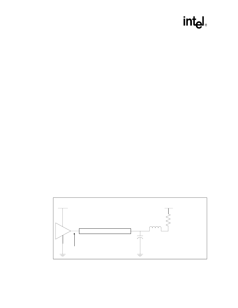
Figure 2-6. Electrical Test Circuit
V
TT
45 ohms, 156 ps/in, 550 mils
L = 2.4nH
C = 1.2pF
V
TT
R
LOAD
= 50 ohms
AC Timings specified at this point
相關(guān)PDF資料 |
PDF描述 |
|---|---|
| 8085AH | 8 BIT HMOS MICROPROCESSORS |
| 8085AH-1 | 8 BIT HMOS MICROPROCESSORS |
| 8085AH-2 | 8 BIT HMOS MICROPROCESSORS |
| 8087 | MATH COPROCESSOR |
| 8087-1 | Circular Connector; MIL SPEC:MIL-DTL-38999 Series III; Body Material:Metal; Series:TV06; No. of Contacts:61; Connector Shell Size:25; Connecting Termination:Crimp; Circular Shell Style:Straight Plug; Body Style:Straight |
相關(guān)代理商/技術(shù)參數(shù) |
參數(shù)描述 |
|---|---|
| 80546KG3200FA | 制造商:undefined 功能描述: |
| 805470 | 制造商:Phoenix Contact 功能描述:Labels Individual Label Polyester White 8x20mm |
| 80-5470-001 | 制造商:Applied Engineering Products (AEP) 功能描述:13"CBL W/CON ON BOTH ENDS - PLUG, R/A PUSHON - Bulk |
| 80547001 | 功能描述:MOTOR 82540 250RPM 220-230V 50/6 制造商:crouzet 系列:* 零件狀態(tài):在售 標(biāo)準(zhǔn)包裝:6 |
| 80547002 | 功能描述:MOTOR 82540 375RPM 220-230V 50HZ 制造商:crouzet 系列:* 零件狀態(tài):在售 標(biāo)準(zhǔn)包裝:6 |
發(fā)布緊急采購(gòu),3分鐘左右您將得到回復(fù)。