- 您現(xiàn)在的位置:買賣IC網(wǎng) > PDF目錄373891 > AD6635BB (ANALOG DEVICES INC) 4-Channel, 80 MSPS WCDMA Receive Signal Processor (RSP) PDF資料下載
參數(shù)資料
| 型號(hào): | AD6635BB |
| 廠商: | ANALOG DEVICES INC |
| 元件分類: | 無繩電話/電話 |
| 英文描述: | 4-Channel, 80 MSPS WCDMA Receive Signal Processor (RSP) |
| 中文描述: | TELECOM, CELLULAR, BASEBAND CIRCUIT, PBGA324 |
| 封裝: | 19 X 19 MM, PLASTIC, BGA-324 |
| 文件頁(yè)數(shù): | 23/60頁(yè) |
| 文件大小: | 799K |
| 代理商: | AD6635BB |
第1頁(yè)第2頁(yè)第3頁(yè)第4頁(yè)第5頁(yè)第6頁(yè)第7頁(yè)第8頁(yè)第9頁(yè)第10頁(yè)第11頁(yè)第12頁(yè)第13頁(yè)第14頁(yè)第15頁(yè)第16頁(yè)第17頁(yè)第18頁(yè)第19頁(yè)第20頁(yè)第21頁(yè)第22頁(yè)當(dāng)前第23頁(yè)第24頁(yè)第25頁(yè)第26頁(yè)第27頁(yè)第28頁(yè)第29頁(yè)第30頁(yè)第31頁(yè)第32頁(yè)第33頁(yè)第34頁(yè)第35頁(yè)第36頁(yè)第37頁(yè)第38頁(yè)第39頁(yè)第40頁(yè)第41頁(yè)第42頁(yè)第43頁(yè)第44頁(yè)第45頁(yè)第46頁(yè)第47頁(yè)第48頁(yè)第49頁(yè)第50頁(yè)第51頁(yè)第52頁(yè)第53頁(yè)第54頁(yè)第55頁(yè)第56頁(yè)第57頁(yè)第58頁(yè)第59頁(yè)第60頁(yè)
REV. 0
AD6635
–23–
INPUT DATA PORTS
The AD6635 features four high speed ADC Input Ports, A, B,
C, and D. The input ports allow for the most flexibility with a
single tuner chip. These can be diversity inputs or truly inde-
pendent inputs such as separate antenna segments. Channels 0
through 3 can take data from either of the input ports A or B
independently. Similarly, Channels 4 through 7 can take data
from either of the Input Ports C or D independently. For added
flexibility, each input port can be used to support multiplexed
inputs, such as found on the AD6600 or other ADCs with multi-
plexed outputs. This added flexibility allows up to eight different
analog sources to be processed simultaneously by the eight
internal AD6635 channels.
In addition, the front end of the AD6635 contains circuitry that
enables high speed signal level detection and control. This is
accomplished with a unique high speed level detection circuit
that offers minimal latency and maximum flexibility to control
up to four analog signal paths. The overall signal path latency
from input to output on the AD6635 can be expressed in high
speed clock cycles. The equation below can be used to calculate
the latency.
=
M
rCIC2
and
M
CIC5
are decimation values for the rCIC2 and CIC5
filters, respectively.
N
TAPS
is the number of RCF taps chosen.
Input Data Format
Each input port consists of a 14-bit mantissa and 3-bit exponent. If
interfacing to a standard ADC, the exponent bits can be grounded.
If connected to a floating point ADC, such as the AD6600, the
exponent bits from that ADC product can be connected to the
input exponent bits of the AD6635. The mantissa data format is
twos complement, and the exponent is unsigned binary.
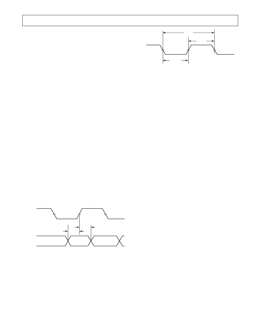
Input Timing
The data from each high speed input port is latched on the
rising edge of CLK. This clock signal is used to sample the
input port and clock the synchronous signal processing stages
that follow in the selected channels.
T
M
M
N
LATENCY
rCIC
CIC
TAPS
+
+
+
2
5
7
26
(
)
CLK
IN[13:0]
EXP[2:0]
DATA
t
SI
t
HI
Figure 24. Input Data Timing Requirements
The clock signals can operate up to 80 MHz and have a 50%
duty cycle. In applications using high speed ADCs, the ADC
sample clock or data valid strobe is typically used to clock the
AD6635.
t
CLKL
t
CLK
t
CLKH
CLKn
Figure 25. CLKn Timing Requirements (n = 0, 1)
Input Enable Control
There are four Input Enable pins IENx (x = A, B, C, or D)
corresponding to individual Input Ports A through D. There are
four modes of operation possible while using each IEN pin.
Using these modes, it is possible to emulate operation of the
other RSPs such as the AD6620, which offer dual channel
modes normally associated with diversity operations. These
modes are IEN transition to Low, IEN transition to High, IEN
High, and Blank on IEN Low.
In the IEN High mode, the inputs and normal operations occur
when the Input Enable is High. In the IEN transition to Low
mode, normal operations occur on the first rising edge of the
clock after the IEN transitions to Low. Likewise in the IEN
transition to High mode, operations occur on the rising edge of
the clock after the IEN transitions to High. See the numerically
Controlled Oscillator section for more details on configuring the
Input Enable Modes. In Blank on IEN Low mode, the input
data is interpreted as zero when IEN is low.
A typical application for input modes would be to take the data
from an AD6600 Diversity ADC to one of the inputs of the
AD6635. The A/B_OUT from that chip would be tied to the
IEN of the corresponding input port. Then one channel within
the AD6635 would be set so that IEN transition to Low is
enabled. Another channel would be configured so that IEN
transition to High is enabled. This would allow two of the
AD6635 channels to be configured to emulate that AD6620 in
diversity mode and receive interleaved input data. Though the
NCO frequencies and other channel characteristics would need
to be set similarly, this feature allows the AD6635 to handle
interleaved data streams such as found on the AD6600.
The difference between the IEN transition to High and the
IEN High is found when a system clock is provided that is
higher than the data rate of the converter. It is often advanta-
geous to supply a clock that runs faster than the data rate so
that additional filter taps can be computed. This indeed leads
to better filtering. To ensure that other parts of the circuit
properly recognize the faster clock in the simplest manner,
the IEN transition to Low or High should be used. In this
mode, only the first clock edge that meets the setup and hold
times will be used to latch and process the input data. All other
clocks pulses are ignored by front end processing. However,
each clock cycle will still produce a new filter computation pair.
Gain Switching
The AD6635 includes circuitry that is useful in applications where
either large dynamic ranges exist, or where gain ranging converters
are employed. This circuitry allows digital thresholds to be set such
that an upper and a lower threshold can be programmed.
One such use of this may be to detect when an ADC is about to
reach full scale with a particular input condition. The results
相關(guān)PDF資料 |
PDF描述 |
|---|---|
| AD6636 | 150 MSPS Wideband Digital Down-Converter (DDC) |
| AD6636BBCZ1 | 150 MSPS Wideband Digital Down-Converter (DDC) |
| AD6636BC | 150 MSPS Wideband Digital Down-Converter (DDC) |
| AD6636CBCZ1 | 150 MSPS Wideband Digital Down-Converter (DDC) |
| AD6636PCB | 150 MSPS Wideband Digital Down-Converter (DDC) |
相關(guān)代理商/技術(shù)參數(shù) |
參數(shù)描述 |
|---|---|
| AD6635BB/PCB | 制造商:Analog Devices 功能描述:Evaluation Kit For 4-Channel, 80MSPS WCDMA Receive Signal Processor |
| AD6635BBZ | 制造商:Analog Devices 功能描述:Receive Signal Processor 324-Pin BGA |
| AD6636 | 制造商:AD 制造商全稱:Analog Devices 功能描述:150 MSPS Wideband Digital Down-Converter (DDC) |
| AD6636BBC | 制造商:Analog Devices 功能描述:Digital Down Converter 256-Pin CSP-BGA |
| AD6636BBCZ | 功能描述:IC DIGITAL DWNCONV 6CH 256CSPBGA RoHS:是 類別:RF/IF 和 RFID >> RF 混頻器 系列:AD6636 產(chǎn)品培訓(xùn)模塊:Lead (SnPb) Finish for COTS Obsolescence Mitigation Program 標(biāo)準(zhǔn)包裝:100 系列:- RF 型:W-CDMA 頻率:2.11GHz ~ 2.17GHz 混頻器數(shù)目:1 增益:17dB 噪音數(shù)據(jù):2.2dB 次要屬性:- 電流 - 電源:11.7mA 電源電壓:2.7 V ~ 3.3 V 包裝:托盤 封裝/外殼:12-VFQFN 裸露焊盤 供應(yīng)商設(shè)備封裝:12-QFN-EP(3x3) |
發(fā)布緊急采購(gòu),3分鐘左右您將得到回復(fù)。