- 您現(xiàn)在的位置:買賣IC網(wǎng) > PDF目錄373891 > AD6635BB (ANALOG DEVICES INC) 4-Channel, 80 MSPS WCDMA Receive Signal Processor (RSP) PDF資料下載
參數(shù)資料
| 型號: | AD6635BB |
| 廠商: | ANALOG DEVICES INC |
| 元件分類: | 無繩電話/電話 |
| 英文描述: | 4-Channel, 80 MSPS WCDMA Receive Signal Processor (RSP) |
| 中文描述: | TELECOM, CELLULAR, BASEBAND CIRCUIT, PBGA324 |
| 封裝: | 19 X 19 MM, PLASTIC, BGA-324 |
| 文件頁數(shù): | 40/60頁 |
| 文件大小: | 799K |
| 代理商: | AD6635BB |
第1頁第2頁第3頁第4頁第5頁第6頁第7頁第8頁第9頁第10頁第11頁第12頁第13頁第14頁第15頁第16頁第17頁第18頁第19頁第20頁第21頁第22頁第23頁第24頁第25頁第26頁第27頁第28頁第29頁第30頁第31頁第32頁第33頁第34頁第35頁第36頁第37頁第38頁第39頁當前第40頁第41頁第42頁第43頁第44頁第45頁第46頁第47頁第48頁第49頁第50頁第51頁第52頁第53頁第54頁第55頁第56頁第57頁第58頁第59頁第60頁
REV. 0
–40–
AD6635
LINK PORT
The AD6635 has four configurable link ports that provide a
seamless data interface with the TigerSHARC DSP. Each link
port allows the AD6635 to write output data to the receive
DMA channel in the TigerSHARC for transfer to memory.
Since they operate independently of each other, each link port
can be connected to a different TigerSHARC or to different link
ports on the same TigerSHARC. Figure 39 shows how to con-
nect one of the four AD6635 link ports to one of the four
TigerSHARC link ports. Individual link ports are configured
through their respective registers.
AD6635
LCLKIN
LCLKOUT
LDAT
PCLK
TigerSHARC
LCLKIN
LCLKOUT
LDAT
PCLK
8
Figure 39. Link Port Connection between AD6635
and TigerSHARC
Link Port Data Format
Each link port can output data to the TigerSHARC in five
different formats: 2-channel, 4-channel, dedicated AGC,
redundant AGC with RSSI word, and redundant AGC without
RSSI word. Each format outputs 2 bytes of I data and 2 bytes of
Q data to form a 4-byte IQ pair. Since the TigerSHARC link
port transfers data in quad-word (16-byte) blocks, four IQ pairs
can make up one quad-word. If the channel data is selected (Bit
0 of 0x1B/0x1D = 0), then 4-byte IQ words of the four channels
can be output in succession, or alternating channel pair IQ
words can be output. Figures 40 and 41 show the quad-word
transmitted for each scenario with corresponding register values
for configuring each link port.
LINK PORT
A OR B
CH 0 I, Q
(4 BYTES)
CH 1 I, Q
(4 BYTES)
CH 2 I, Q
(4 BYTES)
CH 3 I, Q
(4 BYTES)
ADDR 0x1B OR 0x1D BIT 0 = 0, BIT 1 = 0
LINK PORT A
CH 0 I, Q
(4 BYTES)
CH 1 I, Q
(4 BYTES)
CH 0 I, Q
(4 BYTES)
CH 1 I, Q
(4 BYTES)
LINK PORT B
CH 2 I, Q
(4 BYTES)
CH 3 I, Q
(4 BYTES)
CH 2 I, Q
(4 BYTES)
CH 3 I, Q
(4 BYTES)
ADDR 0x1B OR 0x1D BIT 0 = 0, BIT 1 = 1
Figure 40. Link Port Data from RCF
If AGC output is selected (Bit 0 of 0x1B/0x1D = 1), then RSSI
information can be sent with the IQ pair from each AGC. Each
link port can be configured to output data from one AGC or
both link ports can output data from the same AGC. If both link
ports are transmitting the same data, then RSSI information
must be sent with the IQ words (Bit 2 = 0). Note that the actual
AGC RSSI is only 2 bytes (12 bits of RSSI word appended with
four zeros), so the link port sends 2 bytes of 0s immediately after
each RSSI word to make a full 16-byte quad-word.
LINK PORT
A OR B
AGC A I, Q
(4 BYTES)
AGC B I, Q
(4 BYTES)
AGC A I, Q
(4 BYTES)
AGC B I, Q
(4 BYTES)
ADDR 0x1B OR 0x1D BIT 0 = 1, BIT 1 = 0, BIT 2 = 0
LINK PORT
A OR B
AGC A I, Q
(4 BYTES)
AGC A RSSI
(4 BYTES)
AGC B I, Q
(4 BYTES)
AGC B RSSI
(4 BYTES)
ADDR 0x1B OR 0x1D BIT 0 = 1, BIT 1 = 0, BIT 2 = 1
LINK PORT A
AGC A I, Q
(4 BYTES)
AGC A RSSI
(4 BYTES)
AGC A I, Q
(4 BYTES)
AGC A RSSI
(4 BYTES)
AGC B I, Q
(4 BYTES)
AGC B RSSI
(4 BYTES)
AGC B I, Q
(4 BYTES)
AGC B RSSI
(4 BYTES)
LINK PORT B
ADDR 0x1B OR 0x1D BIT 0 = 1, BIT 1 = 1, BIT 2 = 0
Figure 41. Link Port Data from AGC
Note that Bit 0 = 1, Bit 1 = 0, and Bit 2 = 1 is not a valid con-
figuration. Bit 2 must be set to 0 to output AGC A IQ and RSSI
words on link Port A, and AGC B IQ and RSSI words on link
Port B.
Link Port Timing
Link Ports A and B derive their clocks of PCLK0 and link Ports
C and D of PCLK1, which can be externally provided to the
chip (Addr 0x1E, Bit 0 = 0) or generated from the master clock
of the AD6635 (Addr 0x1E, Bit 0 = 1). This register boots to 0
(slave mode) and allows the user to control the data rate coming
from the AD6635. PCLK can be run as fast as 100 MHz.
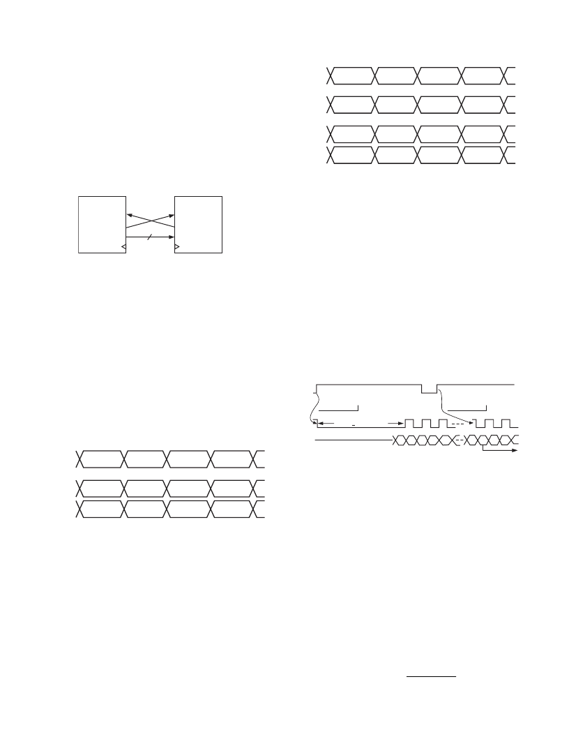
The link port provides 1-byte data-words (Lx[7:0] pins) and
output clocks (LxCLKOUT pins) in response to a ready signal
(LxCLKIN pins) from the receiver, where x = A, B, C, or D.
Each link port transmits 8 bits on each edge of LCLKOUT,
requiring eight LCLKOUT cycles to complete transmission of
the full 16 bytes of a TigerSHARC quad-word.
D0 D1 D2 D3
D4
D15
D0 D1 D2
NEXT QUAD-WORD
TigerSHARC READY TO
RECEIVE QUAD-WORD
WAIT > 6 CYCLES
TigerSHARC READY TO
RECEIVE NEXT QUAD-WORD
LCLKIN
LCLKOUT
LDAT[7:0]
Figure 42. Link Port Data Transfer
Due to the TigerSHARC link port protocol, the AD6635 must
wait at least six PCLK cycles after the TigerSHARC is ready to
receive data, as indicated by the TigerSHARC setting the respec-
tive AD6635 LCLKIN pin high. Once the AD6635 link port
has waited the appropriate number of PCLK cycles and has
begun transmitting data, the TigerSHARC does a connectivity
check by sending the AD6635 LCLKIN low and then high
while the data is being transmitted. This tells the AD6635 link
port that the TigerSHARC’s DMA is ready to receive the next
quad-word after completion of the current quad-word. Because
the connectivity check is done in parallel to the data transmis-
sion, the AD6635 is able to stream uninterrupted data to the
TigerSHARC.
The length of the wait before data transmission is a 4-bit pro-
grammable value in the link port control registers (0x1B and
0x1D, Bits 6–3). This value allows the AD6635 PCLK and the
TigerSHARC PCLK to be run at different rates and out of phase.
WAIT
ceil
f
f
LCLK
LCLK TSHARC
_
≥
¥
ê
ˉ
6
34
_
相關PDF資料 |
PDF描述 |
|---|---|
| AD6636 | 150 MSPS Wideband Digital Down-Converter (DDC) |
| AD6636BBCZ1 | 150 MSPS Wideband Digital Down-Converter (DDC) |
| AD6636BC | 150 MSPS Wideband Digital Down-Converter (DDC) |
| AD6636CBCZ1 | 150 MSPS Wideband Digital Down-Converter (DDC) |
| AD6636PCB | 150 MSPS Wideband Digital Down-Converter (DDC) |
相關代理商/技術參數(shù) |
參數(shù)描述 |
|---|---|
| AD6635BB/PCB | 制造商:Analog Devices 功能描述:Evaluation Kit For 4-Channel, 80MSPS WCDMA Receive Signal Processor |
| AD6635BBZ | 制造商:Analog Devices 功能描述:Receive Signal Processor 324-Pin BGA |
| AD6636 | 制造商:AD 制造商全稱:Analog Devices 功能描述:150 MSPS Wideband Digital Down-Converter (DDC) |
| AD6636BBC | 制造商:Analog Devices 功能描述:Digital Down Converter 256-Pin CSP-BGA |
| AD6636BBCZ | 功能描述:IC DIGITAL DWNCONV 6CH 256CSPBGA RoHS:是 類別:RF/IF 和 RFID >> RF 混頻器 系列:AD6636 產(chǎn)品培訓模塊:Lead (SnPb) Finish for COTS Obsolescence Mitigation Program 標準包裝:100 系列:- RF 型:W-CDMA 頻率:2.11GHz ~ 2.17GHz 混頻器數(shù)目:1 增益:17dB 噪音數(shù)據(jù):2.2dB 次要屬性:- 電流 - 電源:11.7mA 電源電壓:2.7 V ~ 3.3 V 包裝:托盤 封裝/外殼:12-VFQFN 裸露焊盤 供應商設備封裝:12-QFN-EP(3x3) |
發(fā)布緊急采購,3分鐘左右您將得到回復。