- 您現(xiàn)在的位置:買賣IC網(wǎng) > PDF目錄373891 > AD6635BB (ANALOG DEVICES INC) 4-Channel, 80 MSPS WCDMA Receive Signal Processor (RSP) PDF資料下載
參數(shù)資料
| 型號: | AD6635BB |
| 廠商: | ANALOG DEVICES INC |
| 元件分類: | 無繩電話/電話 |
| 英文描述: | 4-Channel, 80 MSPS WCDMA Receive Signal Processor (RSP) |
| 中文描述: | TELECOM, CELLULAR, BASEBAND CIRCUIT, PBGA324 |
| 封裝: | 19 X 19 MM, PLASTIC, BGA-324 |
| 文件頁數(shù): | 33/60頁 |
| 文件大小: | 799K |
| 代理商: | AD6635BB |
第1頁第2頁第3頁第4頁第5頁第6頁第7頁第8頁第9頁第10頁第11頁第12頁第13頁第14頁第15頁第16頁第17頁第18頁第19頁第20頁第21頁第22頁第23頁第24頁第25頁第26頁第27頁第28頁第29頁第30頁第31頁第32頁當前第33頁第34頁第35頁第36頁第37頁第38頁第39頁第40頁第41頁第42頁第43頁第44頁第45頁第46頁第47頁第48頁第49頁第50頁第51頁第52頁第53頁第54頁第55頁第56頁第57頁第58頁第59頁第60頁
REV. 0
AD6635
–33–
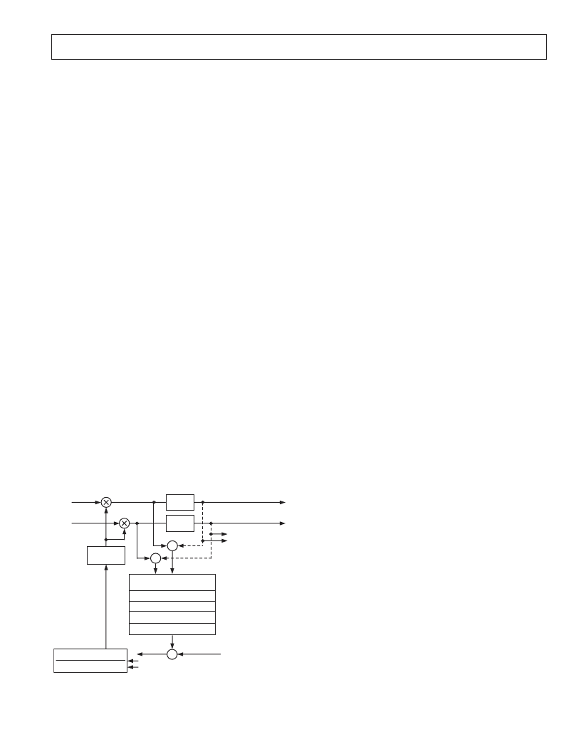
The AGC Loop
The AGC loop is implemented using a log-linear architecture. It
contains four basic operations: power calculation, error calcula-
tion, loop filtering, and gain multiplication.
The AGC can be configured to operate in one of two modes:
Desired Signal Level mode or Desired Clipping Level mode, as
set by Bit 4 of AGC control word (0x0A, 0x12). The AGC adjusts
the gain of the incoming data according to how far it is from a
given desired signal level or desired clipping level, depending on
the mode of operation selected. Two data paths to the AGC
loop are provided: one before the clipping circuitry and one
after the clipping circuitry, as shown in Figure 32. For Desired
Signal Level mode, only the I/Q path from before the clipping is
used. For Desired Clipping Level mode, the difference of the I/Q
signals from before and after the clipping circuitry is used.
Desired Signal Level Mode
In this mode of operation, the AGC strives to maintain the
output signal at a programmable set level. This mode of operation
is selected by putting a value of zero in Bit 4 of AGC control
word (0x0A, 0x12). First, the loop finds the square (or power)
of the incoming complex data signal by squaring I and Q and
adding them. This operation is implemented in exponential
domain using 2x (power of 2).
The AGC loop has an average and decimate block. This average
and decimate operation takes place on power samples and before
the square root operation. This block can be programmed to
average 1–16384 power samples and the decimate section can
be programmed to update the AGC once every 1–4096 samples.
The limitation on the averaging operation is that the number of
averaged power samples should be a multiple of the decimation
value (1, 2, 3, or 4 times).
The averaging and decimation effectively means the AGC can
operate over averaged power of 1–16384 output samples. The
choice of updating the AGC once every 1–4096 samples and
operating on average power facilitates the implementation of a
loop filter with slow time constants, where the AGC error con-
verges slowly and makes infrequent gain adjustments. It would
also be useful in scenarios where the user wants to keep the gain
scaling constant over a frame of data (or a stream of symbols).
CLIP
I
23 BITS
Q
CLIP
MEAN SQUARE (I + jQ)
AVERAGE 1–16384 SAMPLES
DECIMATE 1–4096 SAMPLES
SQUARE ROOT
USED ONLY FOR
DESIRED
CLIPPING LEVEL
MODE
GAIN
MULTIPLIER
I
Q
–
–
2
X
POWER OF 2
Kz
–1
1 – (1 + P)z
–1
+ Pz
–2
ERROR
'K' GAIN
'P' POLE
+
–
'R' DESIRED
PROGRAMMABLE
BIT WIDTH
LOG
2
(X)
Figure 32. Block Diagram of the AGC
Due to the limitation on the number of average samples being a
multiple of the decimation value, only the multiple number 1, 2,
3, or 4 is programmed. This number is programmed in Bits 1, 0
of the 0x10 and 0x18 registers. These averaged samples are then
decimated with decimation ratios programmable from 1 to
4096. This decimation ratio is defined in the 12-bit registers
0x11 and 0x19.
The average and decimate operations are tied together and
implemented using a first-order CIC filter and some FIFO
registers. There is a gain and bit growth associated with CIC
filters, which depend on the decimation ratio. To compensate
for the gain associated with these operations, attenuation scaling
is provided before the CIC filter.
This scaling operation accounts for the division associated with
the averaging operation as well as the traditional bit growth in
CIC filters. Since this scaling is implemented as a bit shift
operation, only coarse scaling is possible. Fine scaling is imple-
mented as an offset in the Request Level explained later. The
attenuation scaling (SCIC) is programmable from 0 to 14 using
four bits of the 0x10 and 0x18 registers and is given by:
[
where
M
CIC
is the decimation ratio (1–4096) and
N
AVG
is the
number of averaged samples programmed as a multiple of the
decimation ratio (1, 2, 3, or 4).
For example if a decimation ratio, M
CIC
, is 1000, and
N
AVG
is
selected to be 3 (decimation of 1000 and averaging of 3000
samples), the actual gain due to averaging and decimation is
3000 or 69.54 dB (= 20 log 3000). Since attenuation is
implemented as a bit shift operation, only multiples of 6.02 dB
attenuations are possible. SCIC in this case is 12, corresponding
to 72.24 dB. This way SCIC scaling always attenuates more
than sufficiently to compensate for the gain changes in the aver-
age and decimate sections, and hence prevents overflows in the
AGC loop. But it is also evident that the CIC scaling is intro-
ducing a gain error (difference between gain due to CIC and
attenuation provided) of up to 6.02 dB. This error should be
compensated for in the Request signal level as explained below.
Logarithm to the base 2 is applied to the output from the aver-
age and decimate section. These decimated power samples (in
logarithmic domain) are converted to rms signal samples by
applying a square root. This square root is implemented using a
simple shift operation. The rms samples so obtained are sub-
tracted from the request signal level ‘R’ specified in registers
(0x0B, 0x14) leaving an error term to be processed by the loop
filter, G(z).
The user sets this programmable request signal level ‘R’ according
to the desired output signal level. The request signal level ‘R’
is programmable from 0 to –23.99 dB in steps of 0.094 dB. The
request signal level should also compensate for any error due to
the CIC scaling as explained previously. Hence, the request
signal level is offset by the amount of error induced in the CIC
given by
(
where, the offset is in dB.
Continuing with the previous example, this offset is given by
72.24 – 69.54 = 2.7 dB. So the request signal level is given by
S
ceil
M
N
CIC
CIC
AVG
=
¥
(
)
]
log
2
Offset
M
N
S
CIC
AVG
CIC
=
¥
)
¥
20
6 02
.
10
log
–
相關PDF資料 |
PDF描述 |
|---|---|
| AD6636 | 150 MSPS Wideband Digital Down-Converter (DDC) |
| AD6636BBCZ1 | 150 MSPS Wideband Digital Down-Converter (DDC) |
| AD6636BC | 150 MSPS Wideband Digital Down-Converter (DDC) |
| AD6636CBCZ1 | 150 MSPS Wideband Digital Down-Converter (DDC) |
| AD6636PCB | 150 MSPS Wideband Digital Down-Converter (DDC) |
相關代理商/技術參數(shù) |
參數(shù)描述 |
|---|---|
| AD6635BB/PCB | 制造商:Analog Devices 功能描述:Evaluation Kit For 4-Channel, 80MSPS WCDMA Receive Signal Processor |
| AD6635BBZ | 制造商:Analog Devices 功能描述:Receive Signal Processor 324-Pin BGA |
| AD6636 | 制造商:AD 制造商全稱:Analog Devices 功能描述:150 MSPS Wideband Digital Down-Converter (DDC) |
| AD6636BBC | 制造商:Analog Devices 功能描述:Digital Down Converter 256-Pin CSP-BGA |
| AD6636BBCZ | 功能描述:IC DIGITAL DWNCONV 6CH 256CSPBGA RoHS:是 類別:RF/IF 和 RFID >> RF 混頻器 系列:AD6636 產(chǎn)品培訓模塊:Lead (SnPb) Finish for COTS Obsolescence Mitigation Program 標準包裝:100 系列:- RF 型:W-CDMA 頻率:2.11GHz ~ 2.17GHz 混頻器數(shù)目:1 增益:17dB 噪音數(shù)據(jù):2.2dB 次要屬性:- 電流 - 電源:11.7mA 電源電壓:2.7 V ~ 3.3 V 包裝:托盤 封裝/外殼:12-VFQFN 裸露焊盤 供應商設備封裝:12-QFN-EP(3x3) |
發(fā)布緊急采購,3分鐘左右您將得到回復。