- 您現(xiàn)在的位置:買賣IC網(wǎng) > PDF目錄373891 > AD6636CBCZ1 (Analog Devices, Inc.) 150 MSPS Wideband Digital Down-Converter (DDC) PDF資料下載
參數(shù)資料
| 型號: | AD6636CBCZ1 |
| 廠商: | Analog Devices, Inc. |
| 元件分類: | 數(shù)字上/下變頻 |
| 英文描述: | 150 MSPS Wideband Digital Down-Converter (DDC) |
| 中文描述: | 150MSPS的寬帶數(shù)字下變頻器(DDC) |
| 文件頁數(shù): | 50/72頁 |
| 文件大?。?/td> | 1629K |
| 代理商: | AD6636CBCZ1 |
第1頁第2頁第3頁第4頁第5頁第6頁第7頁第8頁第9頁第10頁第11頁第12頁第13頁第14頁第15頁第16頁第17頁第18頁第19頁第20頁第21頁第22頁第23頁第24頁第25頁第26頁第27頁第28頁第29頁第30頁第31頁第32頁第33頁第34頁第35頁第36頁第37頁第38頁第39頁第40頁第41頁第42頁第43頁第44頁第45頁第46頁第47頁第48頁第49頁當(dāng)前第50頁第51頁第52頁第53頁第54頁第55頁第56頁第57頁第58頁第59頁第60頁第61頁第62頁第63頁第64頁第65頁第66頁第67頁第68頁第69頁第70頁第71頁第72頁
AD6636
Rev. 0 | Page 50 of 72
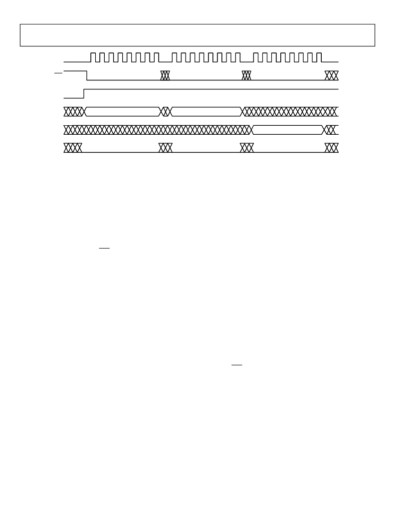
SCLK
SCS
SMODE
SDI
SDO
MODE
INSTRUCTION BYTE 1
INSTRUCTION BYTE 2
VALID OUTPUT
0
Figure 45. SPI Readback Timing
SPORT Mode Write Operation
In SPORT mode, the SCLK runs continuously, and external
SRFS and STFS signals are used for framing of the input and
out words. Incoming framing signals SRFS (receive/input) and
STFS (transmit/output) are valid when they are high for one
SCLK cycle. All input and output data must be transmitted or
received in 8-bit words by using the appropriate framing signals.
During a write cycle, the data is registered on the rising edge of
SCLK. Therefore, the programming device outputs data on the
falling edge of the SCLK. The SCS pin is low for both read and
write cycles.
For a write operation, the user must write two 8-bit instruction
words to the SPORT to instruct the AD6636 internal control
logic about the data to be written. The first instruction word is
an address location. If MSBFIRST is Logic 1, this address is the
ending address; if MSBFIRST is Logic 0, this address is the
starting address. The second instruction word contains a 1-bit
read/write indicator (MSB bit: 1 = read, 0 = write), followed by a
7-bit field to indicate the number of address locations to write
(N). Each write cycle takes nine clock cycles, with SRFS high on
the first clock cycle and the 8-bit instruction word on the next
eight clock cycles.
Following the instruction words is N write operations (each one
byte long), where N is the number of address locations to write.
Each write operation must include SRFS high for one clock
cycle and the 8-bit data. After each write cycle, the internal
address is incremented (MSBFIRST = 0) or decremented
(MSBFIRST = 1). In this case, MSBFIRST indicates the first bit
coming out of or into the SPORT, as well as the byte that is
written first (most significant byte of the N-byte transfer, when
MSBFIRST = 1).
For example, consider writing Addresses 0x01 to 0x07 of
AD6636 register map, when operating in SPORT mode and
MSBFIRST = 0. The instruction words are Addresses 0x01 and
0x07 (MSB = 0 for write).
The following seven write cycles transfer one byte at a time,
sequentially into Addresses 0x01 to 0x07, in that order. The
instruction words and data are written with the LSB first.
If the example is for MSBFIRST = 1, then the instruction words
are 0x07 (Address 7) and 0x07 (the number of addresses to
write). The data corresponds to Addresses 0x07 through to
0x01, in that order. The instruction words and data are
MSB first.
SPORT Mode Read Operation
Data on the SDO pin is shifted out on the positive edge of
SCLK. Therefore, the DSP or other master device registers data
on the falling edge of SCLK. All input and output transfers take
place in 8-bit transactions. The SDO pin is high impedance
when data is not being output.
A read operation is similar to a write operation in its format.
The first two instruction words are written on the SDI pin, the
only difference being that the MSB bit of the second instruction
word is that Logic 1 indicates a read operation. After the
instruction words are written, the master device initiates N read
cycles. Each read cycle consists of an STFS framing signal valid
for one clock cycle and the 8-bit data coming out on the SDO
pin. The SCS pin must be low during the read cycle. Data
corresponding to the addresses to be read is transferred out on
the SDO pin and should be registered by the master device. The
data is MSB first or LSB first, based on the status of the
MSBFIRST pin.
For example, consider reading Addresses 0x01 to 0x07 of
AD6636 register map, when operating in SPORT mode and
MSBFIRST = 0. The instruction words are 0x01 and 0x87
(MSB = 1 for read). The following seven read cycles transfer one
byte at time, sequentially out of Addresses 0x01 to 0x07, in that
order. The instruction words are written LSB first and the data
comes out on the SDO with the LSB first.
相關(guān)PDF資料 |
PDF描述 |
|---|---|
| AD6636PCB | 150 MSPS Wideband Digital Down-Converter (DDC) |
| AD664(中文) | Monolithic 12-Bit Quad DAC(單片12位四D/A轉(zhuǎn)換器) |
| AD6640 | 12-Bit, 65 MSPS IF Sampling A/D Converter |
| AD6640AST | 12-Bit, 65 MSPS IF Sampling A/D Converter |
| AD6640PCB | 12-Bit, 65 MSPS IF Sampling A/D Converter |
相關(guān)代理商/技術(shù)參數(shù) |
參數(shù)描述 |
|---|---|
| AD6636PCB | 制造商:AD 制造商全稱:Analog Devices 功能描述:150 MSPS Wideband Digital Down-Converter (DDC) |
| AD6636XBCZ | 制造商:Analog Devices 功能描述: |
| AD664 | 制造商:AD 制造商全稱:Analog Devices 功能描述:Monolithic 12-Bit Quad DAC |
| AD6640 | 制造商:AD 制造商全稱:Analog Devices 功能描述:12-Bit, 65 MSPS IF Sampling A/D Converter |
| AD6640AST | 制造商:Analog Devices 功能描述:ADC Single Pipelined 65Msps 12-bit Parallel 44-Pin LQFP 制造商:Analog Devices 功能描述:ADC SGL PIPELINED 65MSPS 12-BIT PARALLEL 44LQFP - Trays 制造商:Rochester Electronics LLC 功能描述:12-BIT 65 MSPS MONOLITHIC A/D CONVERTER - Tape and Reel 制造商:Analog Devices 功能描述:Analog-Digital Converter IC Number of Bi |
發(fā)布緊急采購,3分鐘左右您將得到回復(fù)。