- 您現(xiàn)在的位置:買賣IC網(wǎng) > PDF目錄366344 > AM188ER-25KCW (ADVANCED MICRO DEVICES INC) CA-BAYONET PDF資料下載
參數(shù)資料
| 型號: | AM188ER-25KCW |
| 廠商: | ADVANCED MICRO DEVICES INC |
| 元件分類: | 微控制器/微處理器 |
| 英文描述: | CA-BAYONET |
| 中文描述: | 16-BIT, 25 MHz, MICROCONTROLLER, PQFP100 |
| 封裝: | PLASTIC, QFP-100 |
| 文件頁數(shù): | 31/112頁 |
| 文件大小: | 2878K |
| 代理商: | AM188ER-25KCW |
第1頁第2頁第3頁第4頁第5頁第6頁第7頁第8頁第9頁第10頁第11頁第12頁第13頁第14頁第15頁第16頁第17頁第18頁第19頁第20頁第21頁第22頁第23頁第24頁第25頁第26頁第27頁第28頁第29頁第30頁當前第31頁第32頁第33頁第34頁第35頁第36頁第37頁第38頁第39頁第40頁第41頁第42頁第43頁第44頁第45頁第46頁第47頁第48頁第49頁第50頁第51頁第52頁第53頁第54頁第55頁第56頁第57頁第58頁第59頁第60頁第61頁第62頁第63頁第64頁第65頁第66頁第67頁第68頁第69頁第70頁第71頁第72頁第73頁第74頁第75頁第76頁第77頁第78頁第79頁第80頁第81頁第82頁第83頁第84頁第85頁第86頁第87頁第88頁第89頁第90頁第91頁第92頁第93頁第94頁第95頁第96頁第97頁第98頁第99頁第100頁第101頁第102頁第103頁第104頁第105頁第106頁第107頁第108頁第109頁第110頁第111頁第112頁

Am186
TM
ER and Am188
TM
ER Microcontrollers Data Sheet
31
DRAFT
ALE
Address Latch Enable (output, synchronous)
This pin indicates to the system that an address ap-
pears on the address and data bus (AD15–AD0 for
the Am186ER microcontroller or AO15–AO8 and
AD7–AD0 for the Am188ER microcontroller). The ad-
dress is guaranteed valid on the trailing edge of ALE.
This pin is three-stated during ONCE mode.
ARDY
Asynchronous Ready (input, asynchronous,
level-sensitive)
This pin indicates to the microcontroller that the ad-
dressed memory space or I/O device will complete a
data transfer. The ARDY pin accepts a rising edge that
is asynchronous to CLKOUTA and is active High. The
falling edge of ARDY must be synchronized to
CLKOUTA. To always assert the ready condition to the
microcontroller, tie ARDY High. If the system does not
use ARDY, tie the pin Low to yield control to SRDY.
BHE/ADEN
(Am186ER Microcontroller Only)
Bus High Enable (three-state, output, synchronous)
Address Enable (input, internal pullup)
BHE
—During a memory access, this pin and the least-
significant address bit (AD0 or A0) indicate to the sys-
tem which bytes of the data bus (upper, lower, or both)
participate in a bus cycle. The BHE/ADEN and AD0
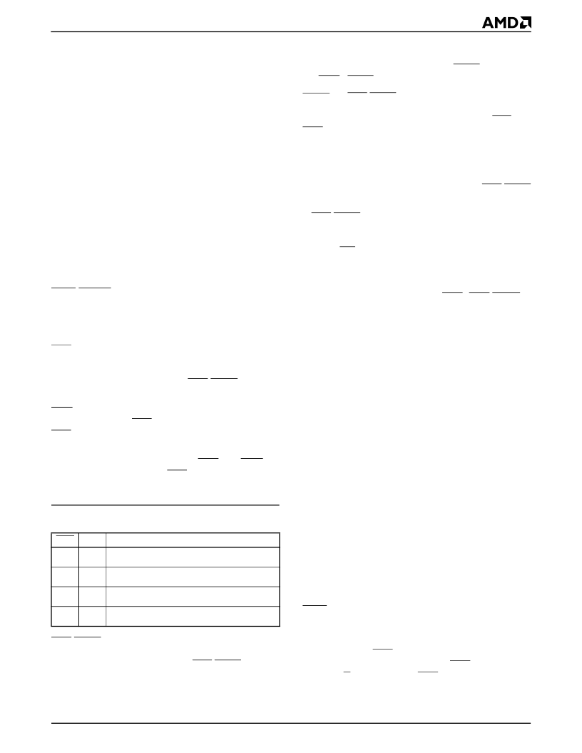
pins are encoded as shown in Table 2.
BHE is asserted during t
1
and remains asserted
through t
3
and t
W
. BHE does not need to be latched.
BHE is three-stated during bus hold and reset condi-
tions.
On the Am186ER microcontroller, WLB and WHB im-
plement the functionality of BHE and AD0 for high and
low byte write enables.
Table 2.
Data Byte Encoding
BHE/ADEN also signals DRAM refresh cycles when
using the multiplexed address and data (AD) bus. A re-
fresh cycle is indicated when both BHE/ADEN and AD0
are High. During refresh cycles, the A bus and the AD
bus are not guaranteed to provide the same address
during the address phase of the AD bus cycle. For this
reason, the A0 signal cannot be used in place of the
AD0 signal to determine refresh cycles. PSRAM re-
freshes also provide an additional RFSH signal (see
the MCS3/RFSH pin description on page 33).
ADEN
—If BHE/ADEN is held High or left floating dur-
ing power-on reset, the address portion of the AD bus
(AD15–AD0) is enabled or disabled during LCS and
UCS bus cycles based on the DA bit in the LMCS and
UMCS registers. If the DA bit is set, the memory ad-
dress is accessed on the A19–A0 pins. This mode of
operation reduces power consumption. For more infor-
mation, see the Bus Operation section on page 41.
There is a weak internal pullup resistor on BHE/ADEN
If BHE/ADEN is held Low on power-on reset, the AD
bus drives both addresses and data. Changing the DA
bit of the LMCS and UMCS registers will have no effect.
(S6 and UZI also assume their normal functionality in
this instance. The PIO Mode and Direction registers
cannot reconfigure these pins as PIOs. See Table 3 on
page 36.) The pin is sampled within three crystal clock
cycles after the rising edge of RES. BHE/ADEN is
three-stated during bus holds and ONCE mode.
Note:
Once the above modes are set, they can be
changed only by resetting the processor.
CLKOUTA
Clock Output A (output, synchronous)
This pin supplies the internal clock to the system. De-
pending on the value of the Power-Save Control Regis-
ter (PDCON), CLKOUTA operates at either the CPU
fundamental frequency (which varies with the divide by
two, times one, and times four clocking modes), the
power-save frequency, or is three-stated (see Figure 10
on page 48). CLKOUTA remains active during reset
and bus hold conditions.
CLKOUTB
Clock Output B (output, synchronous)
This pin supplies a clock to the system. Depending on
the value of the Power-Save Control Register (PD-
CON), CLKOUTB operates at either the CPU funda-
mental frequency (which varies with the divide by two,
times one, and times four clocking modes), the power-
save frequency, or is three-stated (see Figure 10 on
page 48). CLKOUTB remains active during reset and
bus hold conditions.
DEN/PIO5
Data Enable (output, three-state, synchronous)
This pin supplies an output enable to an external data-
bus transceiver. DEN is asserted during memory, I/O,
and interrupt acknowledge cycles. DEN is deasserted
when DT/R changes state. DEN is three-stated during
a bus hold or reset condition.
BHE
AD0 Type of Bus Cycle
0
0
Word Transfer
0
1
High Byte Transfer (Bits 15–8)
1
0
Low Byte Transfer (Bits 7–0)
1
1
Refresh
相關(guān)PDF資料 |
PDF描述 |
|---|---|
| AM20E-2402SC | 20 watt dc-dc converters |
| AM20E-2403SC | 20 watt dc-dc converters |
| AM20E-2405SC | 20 watt dc-dc converters |
| AM20E-4802SC | 20 watt dc-dc converters |
| AM20E-4803SC | 20 watt dc-dc converters |
相關(guān)代理商/技術(shù)參數(shù) |
參數(shù)描述 |
|---|---|
| AM188ER-25KI/W | 制造商:未知廠家 制造商全稱:未知廠家 功能描述:16-Bit Microprocessor |
| AM188ER-25KIW | 制造商:Advanced Micro Devices 功能描述:MCU 16-bit E86 CISC ROMLess 3.3V 100-Pin PQFP 制造商:AMD (Advanced Micro Devices) 功能描述:MCU 16-bit E86 CISC ROMLess 3.3V 100-Pin PQFP |
| AM188ER-25VC/W | 制造商:未知廠家 制造商全稱:未知廠家 功能描述:16-Bit Microprocessor |
| AM188ER-25VCW | 制造商:AMD 制造商全稱:Advanced Micro Devices 功能描述:High-Performance, 80C186- and 80C188-Compatible, 16-Bit Embedded Microcontrollers with RAM |
| AM188ER-25VD\\W | 制造商:Advanced Micro Devices 功能描述: |
發(fā)布緊急采購,3分鐘左右您將得到回復。