- 您現(xiàn)在的位置:買(mǎi)賣(mài)IC網(wǎng) > PDF目錄375996 > GC3011-CQ PDF資料下載
參數(shù)資料
| 型號(hào): | GC3011-CQ |
| 文件頁(yè)數(shù): | 11/34頁(yè) |
| 文件大小: | 194K |
| 代理商: | GC3011-CQ |
第1頁(yè)第2頁(yè)第3頁(yè)第4頁(yè)第5頁(yè)第6頁(yè)第7頁(yè)第8頁(yè)第9頁(yè)第10頁(yè)當(dāng)前第11頁(yè)第12頁(yè)第13頁(yè)第14頁(yè)第15頁(yè)第16頁(yè)第17頁(yè)第18頁(yè)第19頁(yè)第20頁(yè)第21頁(yè)第22頁(yè)第23頁(yè)第24頁(yè)第25頁(yè)第26頁(yè)第27頁(yè)第28頁(yè)第29頁(yè)第30頁(yè)第31頁(yè)第32頁(yè)第33頁(yè)第34頁(yè)

GRAYCHIP,INC.
- 11 -
JULY 22, 1996
GC3011 DIGITAL RESAMPLER
This document contains information which may be changed at any time without notice
The PLL uses a third order loop to reduce jitter due to voltage across R while the pump current is
active. The third order loop is accomplished using a second capacitor C
2
, which should be significantly
smaller than C
1
. Generally, C
2
= C
1
/ 100
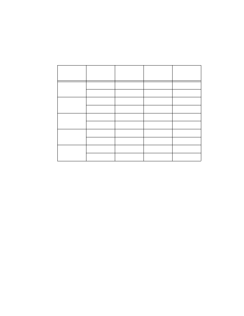
Suggested values for R, C
1
and C
2
are shown in Table 1:
2.8.5
External Output Clock Mode
The FIFO output can be clocked using an externally provided clock. Samples will be output from
the chip synchronous to the rising edge of this clock. This mode is used when the user has an external
output clock, or when multiple chips are being synchronized to an output clock generated by one of a bank
of resampler chips. In this mode the OCK clock pin is driven by the external clock.
2.9
POWER DOWN MODES
The chip has a power down and keep alive circuit. This circuit contains a slow, nominally 1 KHz,
oscillator and a clock-loss detect cell. This circuit is used to detect the loss of clock and provide a slow
keep-alive clock to the chip. The circuit is also used to power down the chip by switching from the high speed
input clock to the low speed keep-alive clock. The low speed clock rate is slow enough to power down the
chip while fast enough to refresh the dynamic nodes within the chip. The user can select whether this circuit
is in the automatic clock-loss detect mode, is always on (power down mode), or is disabled (the slow clock
never kicks in).
Table 1: Suggested PLL Filter Components
F
OUT
(MHZ)
Loop BW
(% of F
OUT
)
R
(Ohms)
C
1
(
μ
F)
C
2
(
μ
F)
1
1
125
3.0
0.03
10
1250
0.03
0.0003
10
1
125
0.3
0.003
10
1250
0.003
0.00003
20
1
125
0.2
0.002
10
1250
0.002
0.00002
40
1
125
0.08
0.0008
10
1250
0.0008
0.000008
60
1
125
0.05
0.0005
10
1250
0.0005
0.000005
相關(guān)PDF資料 |
PDF描述 |
|---|---|
| GC509 | GC509 - Class A Amplifier with 3 Independent Gain Blocks |
| GC509MCRO | Analog IC |
| GC509MINI | Analog IC |
| GC509PLID | Analog IC |
| GC509SLT | Analog IC |
相關(guān)代理商/技術(shù)參數(shù) |
參數(shù)描述 |
|---|---|
| GC3011-PQ | 制造商:Rochester Electronics LLC 功能描述:- Bulk |
| GC3021 | 制造商:TI 制造商全稱(chēng):Texas Instruments 功能描述:MIXER AND CARRIER REMOVAL CHIP |
| GC3021A | 制造商:TI 制造商全稱(chēng):Texas Instruments 功能描述:3.3V MIXER AND CARRIER REMOVAL CHIP |
| GC3021A-PQ | 功能描述:調(diào)節(jié)器/解調(diào)器 Mixer/Carrier Remover RoHS:否 制造商:Texas Instruments 封裝 / 箱體:PVQFN-N24 封裝:Reel |
| GC3021-PQ | 制造商:Rochester Electronics LLC 功能描述:- Bulk |
發(fā)布緊急采購(gòu),3分鐘左右您將得到回復(fù)。