- 您現(xiàn)在的位置:買賣IC網(wǎng) > PDF目錄229297 > MT48LC4M16A2P-75:G 4M X 16 SYNCHRONOUS DRAM, 5.4 ns, PDSO54 PDF資料下載
參數(shù)資料
| 型號: | MT48LC4M16A2P-75:G |
| 元件分類: | DRAM |
| 英文描述: | 4M X 16 SYNCHRONOUS DRAM, 5.4 ns, PDSO54 |
| 封裝: | 0.400 INCH, ROHS COMPLIANT, PLASTIC, TSOP2-54 |
| 文件頁數(shù): | 22/72頁 |
| 文件大?。?/td> | 3455K |
第1頁第2頁第3頁第4頁第5頁第6頁第7頁第8頁第9頁第10頁第11頁第12頁第13頁第14頁第15頁第16頁第17頁第18頁第19頁第20頁第21頁當(dāng)前第22頁第23頁第24頁第25頁第26頁第27頁第28頁第29頁第30頁第31頁第32頁第33頁第34頁第35頁第36頁第37頁第38頁第39頁第40頁第41頁第42頁第43頁第44頁第45頁第46頁第47頁第48頁第49頁第50頁第51頁第52頁第53頁第54頁第55頁第56頁第57頁第58頁第59頁第60頁第61頁第62頁第63頁第64頁第65頁第66頁第67頁第68頁第69頁第70頁第71頁第72頁
PDF: 09005aef80725c0b/Source: 09005aef806fc13c
Micron Technology, Inc., reserves the right to change products or specifications without notice.
64MSDRAM_2.fm - Rev. N 12/08 EN
29
2000 Micron Technology, Inc. All rights reserved.
64Mb: x4, x8, x16 SDRAM
Commands
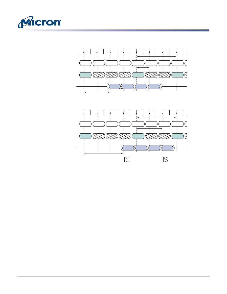
Figure 17:
Terminating a READ Burst
Note:
DQM is LOW.
WRITEs
WRITE bursts are initiated with a WRITE command, as shown in Figure 18 on page 30.
The starting column and bank addresses are provided with the WRITE command, and
auto precharge is either enabled or disabled for that access. If auto precharge is enabled,
the row being accessed is precharged at the completion of the burst. For the generic
WRITE commands used in the following illustrations, auto precharge is disabled.
During WRITE bursts, the first valid data-in element will be registered coincident with
the WRITE command. Subsequent data elements will be registered on each successive
positive clock edge. Upon completion of a fixed-length burst, assuming no other
commands have been initiated, the DQs will remain High-Z, and any additional input
data will be ignored (see Figure 19 on page 30). A full-page burst will continue until
terminated. (At the end of the page, it will wrap to column 0 and continue.)
Data for any WRITE burst may be truncated with a subsequent WRITE command, and
data for a fixed-length WRITE burst may be immediately followed by data for a WRITE
command. The new WRITE command can be issued on any clock following the previous
WRITE command, and the data provided coincident with the new command applies to
the new command.
DON’T CARE
CLK
DQ
DOUT
n
T2
T1
T4
T3
T6
T5
T0
COMMAND
ADDRESS
READ
NOP
DOUT
n + 1
DOUT
n + 2
DOUT
n + 3
BURST
TERMINATE
ACTIVE
t RP
T7
CLK
DQ
DOUT
n
T2
T1
T4
T3
T6
T5
T0
COMMAND
ADDRESS
READ
NOP
DOUT
n + 1
DOUT
n + 2
DOUT
n + 3
BURST
TERMINATE
ACTIVE
t RP
T7
X = 1 cycle
CL = 2
CL = 3
X = 2 cycles
BANK a,
COL n
BANK a,
ROW
BANK
(a or all)
BANK a,
COL n
BANK a,
ROW
BANK
(a or all)
TRANSITIONING DATA
相關(guān)PDF資料 |
PDF描述 |
|---|---|
| M93C06-MB6G | 16 X 16 MICROWIRE BUS SERIAL EEPROM, DSO8 |
| MT48LC4M16A2F4-6IT:G | 4M X 16 SYNCHRONOUS DRAM, 5.5 ns, PBGA54 |
| MT46V32M8FG-6TIT:G | 32M X 8 DDR DRAM, 0.7 ns, PBGA60 |
| MT46V32M8BG-6AT:G | 32M X 8 DDR DRAM, 0.7 ns, PBGA60 |
| M29F800FB55N3E2 | 512K X 16 FLASH 5V PROM, 55 ns, PDSO48 |
相關(guān)代理商/技術(shù)參數(shù) |
參數(shù)描述 |
|---|---|
| MT48LC4M16A2P75ITG | 制造商:Micron Technology Inc 功能描述: |
| MT48LC4M16A2P-75ITG | 制造商: 功能描述: |
| MT48LC4M16A2P-7E | 制造商:Micron Technology Inc 功能描述:SDRAM 64MBIT 133MHZ 54TSOP 制造商:Micron Technology Inc 功能描述:SDRAM, 64MBIT, 133MHZ, 54TSOP 制造商:Micron Technology Inc 功能描述:SDRAM, 64MBIT, 133MHZ, 54TSOP, Memory Type:DRAM - Synchronous, Memory Configurat |
發(fā)布緊急采購,3分鐘左右您將得到回復(fù)。