- 您現(xiàn)在的位置:買賣IC網(wǎng) > PDF目錄229297 > MT48LC4M16A2P-75:G 4M X 16 SYNCHRONOUS DRAM, 5.4 ns, PDSO54 PDF資料下載
參數(shù)資料
| 型號(hào): | MT48LC4M16A2P-75:G |
| 元件分類: | DRAM |
| 英文描述: | 4M X 16 SYNCHRONOUS DRAM, 5.4 ns, PDSO54 |
| 封裝: | 0.400 INCH, ROHS COMPLIANT, PLASTIC, TSOP2-54 |
| 文件頁數(shù): | 46/72頁 |
| 文件大?。?/td> | 3455K |
第1頁第2頁第3頁第4頁第5頁第6頁第7頁第8頁第9頁第10頁第11頁第12頁第13頁第14頁第15頁第16頁第17頁第18頁第19頁第20頁第21頁第22頁第23頁第24頁第25頁第26頁第27頁第28頁第29頁第30頁第31頁第32頁第33頁第34頁第35頁第36頁第37頁第38頁第39頁第40頁第41頁第42頁第43頁第44頁第45頁當(dāng)前第46頁第47頁第48頁第49頁第50頁第51頁第52頁第53頁第54頁第55頁第56頁第57頁第58頁第59頁第60頁第61頁第62頁第63頁第64頁第65頁第66頁第67頁第68頁第69頁第70頁第71頁第72頁
PDF: 09005aef80725c0b/Source: 09005aef806fc13c
Micron Technology, Inc., reserves the right to change products or specifications without notice.
64MSDRAM_2.fm - Rev. N 12/08 EN
50
2000 Micron Technology, Inc. All rights reserved.
64Mb: x4, x8, x16 SDRAM
Notes
1. All voltages referenced to VSS.
2. This parameter is sampled. VDD, VDDQ = +3.3V; f = 1 MHz, TA = 25°C; pin under test
biased at 1.4V.
3. IDD is dependent on output loading and cycle rates. Specified values are obtained
with minimum cycle time and the outputs open.
4. Enables on-chip refresh and address counters.
5. The minimum specifications are used only to indicate cycle time at which proper
operation over the full temperature range (0°C ≤ TA ≤ +70°C (commercial), –40°C ≤ TA
≤ +85°C (industrial), and –40°C ≤ T
A ≤ +105°C (automotive) is ensured.
6. An initial pause of 100s is required after power-up, followed by two AUTO REFRESH
commands, before proper device operation is ensured. (VDD and VDDQ must be pow-
ered up simultaneously. VSS and VSSQ must be at same potential.) The two AUTO
REFRESH command wake-ups should be repeated any time the tREF refresh require-
ment is exceeded.
7. AC characteristics assume tT = 1ns.
8. In addition to meeting the transition rate specification, the clock and CKE must tran-
sit between VIH and VIL (or between VIL and VIH) in a monotonic manner.
9. Outputs measured at 1.5V with equivalent load:
10. tHZ defines the time at which the output achieves the open circuit condition; it is not
a reference to VOH or VOL. The last valid data element will meet tOH before going
High-Z.
11. C timing and IDD tests have VIL = 0V and VIH = 3V, with timing referenced to 1.5V
crossover point. If the input transition time is longer than 1 ns, then the timing is ref-
erenced at VIL (MAX) and VIH (MIN) and no longer at the 1.5V crossover point. CLK
should always be 1.5V referenced to crossover. Refer to Micron technical note
12. Other input signals are allowed to transition no more than once every two clocks and
are otherwise at valid VIH or VIL levels.
13. IDD specifications are tested after the device is properly initialized.
14. Timing actually specified by tCKS; clock(s) specified as a reference only at minimum
cycle rate.
15. Timing actually specified by tWR plus tRP; clock(s) specified as a reference only at
minimum cycle rate.
16. Timing actually specified by tWR.
17. Required clocks are specified by JEDEC functionality and are not dependent on any
timing parameter.
18. The IDD current will increase or decrease proportionally according to the amount of
frequency alteration for the test condition.
19. Address transitions average one transition every two clocks.
20. CLK must be toggled a minimum of two times during this period.
21. Based on tCK = 7.5ns for -75 and -7E, tCK = 6ns for -6.
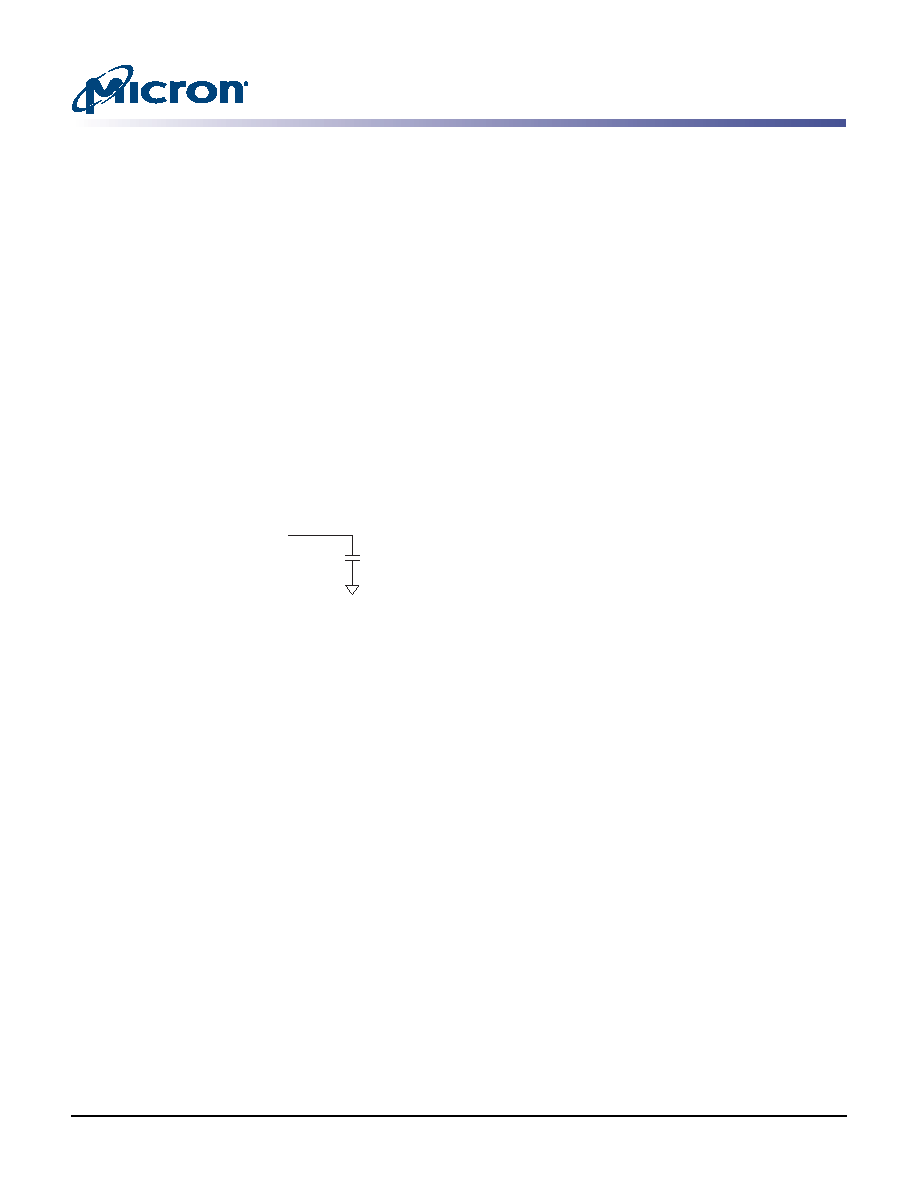
Q
50pF
相關(guān)PDF資料 |
PDF描述 |
|---|---|
| M93C06-MB6G | 16 X 16 MICROWIRE BUS SERIAL EEPROM, DSO8 |
| MT48LC4M16A2F4-6IT:G | 4M X 16 SYNCHRONOUS DRAM, 5.5 ns, PBGA54 |
| MT46V32M8FG-6TIT:G | 32M X 8 DDR DRAM, 0.7 ns, PBGA60 |
| MT46V32M8BG-6AT:G | 32M X 8 DDR DRAM, 0.7 ns, PBGA60 |
| M29F800FB55N3E2 | 512K X 16 FLASH 5V PROM, 55 ns, PDSO48 |
相關(guān)代理商/技術(shù)參數(shù) |
參數(shù)描述 |
|---|---|
| MT48LC4M16A2P75ITG | 制造商:Micron Technology Inc 功能描述: |
| MT48LC4M16A2P-75ITG | 制造商: 功能描述: |
| MT48LC4M16A2P-7E | 制造商:Micron Technology Inc 功能描述:SDRAM 64MBIT 133MHZ 54TSOP 制造商:Micron Technology Inc 功能描述:SDRAM, 64MBIT, 133MHZ, 54TSOP 制造商:Micron Technology Inc 功能描述:SDRAM, 64MBIT, 133MHZ, 54TSOP, Memory Type:DRAM - Synchronous, Memory Configurat |
發(fā)布緊急采購(gòu),3分鐘左右您將得到回復(fù)。