- 您現(xiàn)在的位置:買賣IC網(wǎng) > PDF目錄229297 > MT48LC4M16A2P-75:G 4M X 16 SYNCHRONOUS DRAM, 5.4 ns, PDSO54 PDF資料下載
參數(shù)資料
| 型號: | MT48LC4M16A2P-75:G |
| 元件分類: | DRAM |
| 英文描述: | 4M X 16 SYNCHRONOUS DRAM, 5.4 ns, PDSO54 |
| 封裝: | 0.400 INCH, ROHS COMPLIANT, PLASTIC, TSOP2-54 |
| 文件頁數(shù): | 31/72頁 |
| 文件大小: | 3455K |
第1頁第2頁第3頁第4頁第5頁第6頁第7頁第8頁第9頁第10頁第11頁第12頁第13頁第14頁第15頁第16頁第17頁第18頁第19頁第20頁第21頁第22頁第23頁第24頁第25頁第26頁第27頁第28頁第29頁第30頁當前第31頁第32頁第33頁第34頁第35頁第36頁第37頁第38頁第39頁第40頁第41頁第42頁第43頁第44頁第45頁第46頁第47頁第48頁第49頁第50頁第51頁第52頁第53頁第54頁第55頁第56頁第57頁第58頁第59頁第60頁第61頁第62頁第63頁第64頁第65頁第66頁第67頁第68頁第69頁第70頁第71頁第72頁
PDF: 09005aef80725c0b/Source: 09005aef806fc13c
Micron Technology, Inc., reserves the right to change products or specifications without notice.
64MSDRAM_2.fm - Rev. N 12/08 EN
37
2000 Micron Technology, Inc. All rights reserved.
64Mb: x4, x8, x16 SDRAM
Commands
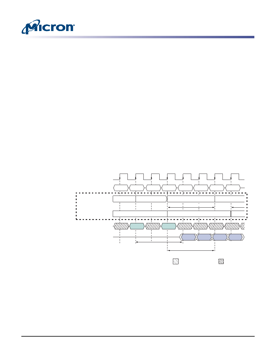
READ with Auto Precharge
Interrupted by a READ (with or without auto precharge): A READ to bank m will inter-
rupt a READ on bank n, CL later. The precharge to bank n will begin when the READ
to bank m is registered (Figure 29 on page 37).
Interrupted by a WRITE (with or without auto precharge): A WRITE to bank m will
interrupt a READ on bank n when registered. DQM should be used two clocks prior to
the WRITE command to prevent bus contention. The precharge to bank n will begin
when the WRITE to bank m is registered (Figure 30 on page 38).
WRITE with Auto Precharge
Interrupted by a READ (with or without auto precharge): A READ to bank m will inter-
rupt a WRITE on bank n when registered, with the data-out appearing CL later. The
precharge to bank n will begin after tWR is met, where tWR begins when the READ to
bank m is registered. The last valid WRITE to bank n will be data-in registered one
clock prior to the READ to bank m (Figure 31 on page 38).
Interrupted by a WRITE (with or without auto precharge): A WRITE to bank m will
interrupt a WRITE on bank n when registered. The precharge to bank n will begin
after tWR is met, where tWR begins when the WRITE to bank m is registered. The last
valid data WRITE to bank n will be data registered one clock prior to a WRITE to bank
Figure 29:
READ With Auto Precharge Interrupted by a READ
Note:
DQM is LOW.
DON’T CARE
CLK
DQ
DOUT
a
T2
T1
T4
T3
T6
T5
T0
COMMAND
READ - AP
BANK n
NOP
DOUT
a + 1
DOUT
d
DOUT
d + 1
NOP
T7
BANK n
CAS Latency = 3 (BANK m)
BANK m
ADDRESS
Idle
NOP
BANK n,
COL a
BANK m,
COL d
READ - AP
BANK m
Internal
States
t
Page Active
READ with Burst of 4
Interrupt Burst, Precharge
Page Active
READ with Burst of 4
Precharge
RP - BANK n
tRP - BANK m
CAS Latency = 3 (BANK n)
TRANSITIONING DATA
相關(guān)PDF資料 |
PDF描述 |
|---|---|
| M93C06-MB6G | 16 X 16 MICROWIRE BUS SERIAL EEPROM, DSO8 |
| MT48LC4M16A2F4-6IT:G | 4M X 16 SYNCHRONOUS DRAM, 5.5 ns, PBGA54 |
| MT46V32M8FG-6TIT:G | 32M X 8 DDR DRAM, 0.7 ns, PBGA60 |
| MT46V32M8BG-6AT:G | 32M X 8 DDR DRAM, 0.7 ns, PBGA60 |
| M29F800FB55N3E2 | 512K X 16 FLASH 5V PROM, 55 ns, PDSO48 |
相關(guān)代理商/技術(shù)參數(shù) |
參數(shù)描述 |
|---|---|
| MT48LC4M16A2P75ITG | 制造商:Micron Technology Inc 功能描述: |
| MT48LC4M16A2P-75ITG | 制造商: 功能描述: |
| MT48LC4M16A2P-7E | 制造商:Micron Technology Inc 功能描述:SDRAM 64MBIT 133MHZ 54TSOP 制造商:Micron Technology Inc 功能描述:SDRAM, 64MBIT, 133MHZ, 54TSOP 制造商:Micron Technology Inc 功能描述:SDRAM, 64MBIT, 133MHZ, 54TSOP, Memory Type:DRAM - Synchronous, Memory Configurat |
發(fā)布緊急采購,3分鐘左右您將得到回復。