- 您現(xiàn)在的位置:買(mǎi)賣(mài)IC網(wǎng) > PDF目錄359352 > VCT3801A (MICRONAS SEMICONDUCTOR HOLDING AG) Video/Controller/Teletext IC Family PDF資料下載
參數(shù)資料
| 型號(hào): | VCT3801A |
| 廠商: | MICRONAS SEMICONDUCTOR HOLDING AG |
| 英文描述: | Video/Controller/Teletext IC Family |
| 中文描述: | 視頻/控制/圖文電視IC系列 |
| 文件頁(yè)數(shù): | 125/172頁(yè) |
| 文件大?。?/td> | 2243K |
| 代理商: | VCT3801A |
第1頁(yè)第2頁(yè)第3頁(yè)第4頁(yè)第5頁(yè)第6頁(yè)第7頁(yè)第8頁(yè)第9頁(yè)第10頁(yè)第11頁(yè)第12頁(yè)第13頁(yè)第14頁(yè)第15頁(yè)第16頁(yè)第17頁(yè)第18頁(yè)第19頁(yè)第20頁(yè)第21頁(yè)第22頁(yè)第23頁(yè)第24頁(yè)第25頁(yè)第26頁(yè)第27頁(yè)第28頁(yè)第29頁(yè)第30頁(yè)第31頁(yè)第32頁(yè)第33頁(yè)第34頁(yè)第35頁(yè)第36頁(yè)第37頁(yè)第38頁(yè)第39頁(yè)第40頁(yè)第41頁(yè)第42頁(yè)第43頁(yè)第44頁(yè)第45頁(yè)第46頁(yè)第47頁(yè)第48頁(yè)第49頁(yè)第50頁(yè)第51頁(yè)第52頁(yè)第53頁(yè)第54頁(yè)第55頁(yè)第56頁(yè)第57頁(yè)第58頁(yè)第59頁(yè)第60頁(yè)第61頁(yè)第62頁(yè)第63頁(yè)第64頁(yè)第65頁(yè)第66頁(yè)第67頁(yè)第68頁(yè)第69頁(yè)第70頁(yè)第71頁(yè)第72頁(yè)第73頁(yè)第74頁(yè)第75頁(yè)第76頁(yè)第77頁(yè)第78頁(yè)第79頁(yè)第80頁(yè)第81頁(yè)第82頁(yè)第83頁(yè)第84頁(yè)第85頁(yè)第86頁(yè)第87頁(yè)第88頁(yè)第89頁(yè)第90頁(yè)第91頁(yè)第92頁(yè)第93頁(yè)第94頁(yè)第95頁(yè)第96頁(yè)第97頁(yè)第98頁(yè)第99頁(yè)第100頁(yè)第101頁(yè)第102頁(yè)第103頁(yè)第104頁(yè)第105頁(yè)第106頁(yè)第107頁(yè)第108頁(yè)第109頁(yè)第110頁(yè)第111頁(yè)第112頁(yè)第113頁(yè)第114頁(yè)第115頁(yè)第116頁(yè)第117頁(yè)第118頁(yè)第119頁(yè)第120頁(yè)第121頁(yè)第122頁(yè)第123頁(yè)第124頁(yè)當(dāng)前第125頁(yè)第126頁(yè)第127頁(yè)第128頁(yè)第129頁(yè)第130頁(yè)第131頁(yè)第132頁(yè)第133頁(yè)第134頁(yè)第135頁(yè)第136頁(yè)第137頁(yè)第138頁(yè)第139頁(yè)第140頁(yè)第141頁(yè)第142頁(yè)第143頁(yè)第144頁(yè)第145頁(yè)第146頁(yè)第147頁(yè)第148頁(yè)第149頁(yè)第150頁(yè)第151頁(yè)第152頁(yè)第153頁(yè)第154頁(yè)第155頁(yè)第156頁(yè)第157頁(yè)第158頁(yè)第159頁(yè)第160頁(yè)第161頁(yè)第162頁(yè)第163頁(yè)第164頁(yè)第165頁(yè)第166頁(yè)第167頁(yè)第168頁(yè)第169頁(yè)第170頁(yè)第171頁(yè)第172頁(yè)
ADVANCE INFORMATION
VCT 38xxA
Micronas
125
5.17.5.ADC Registers
A write access to register AD0 starts the A/D conver-
sion of the written channel number and sampling dura-
tion. The flag EOC signals the end of conversion. The
result is stored in register AD1 (bit 9 to 2) and in regis-
ter AD0 (bit 1 and 0).
EOC
r1:
r0:
End of Conversion
End of conversion
Busy
EOC is reset by a write access to the register AD0.
EOC must be true before starting the first conversion
after enabling the module by setting SR1.ADC.
CMPO
r1:
r0:
Comparator Output
Input is lower than reference voltage.
Input is higher than reference voltage.
TSAMP
Sampling Time
TSAMP adjusts the sample time and the conversion
time. The total conversion time is 20 clock cycles
longer than the sample time. Sampling starts one clock
cycle after completion of the write access to AD0.
CHANNEL Channel of Input Multiplexer
CHANNEL selects from which port pin the conversion
is done. The MSB of CHANNEL is bit 3. No port pin is
connected to the ADC if the channel 0 is selected. In
this case the input of the A/D converter is connected to
ground. After reset, CHANNEL is set to zero.
AN 9 to 0
Analog Value Bit 9 to 0
The 10 bit analog value is in the range of 0 to 1023.
The 8 MSB can be read from register AD1. The two
LSB can be read from register AD0. The result is avail-
able until a new conversion is started.
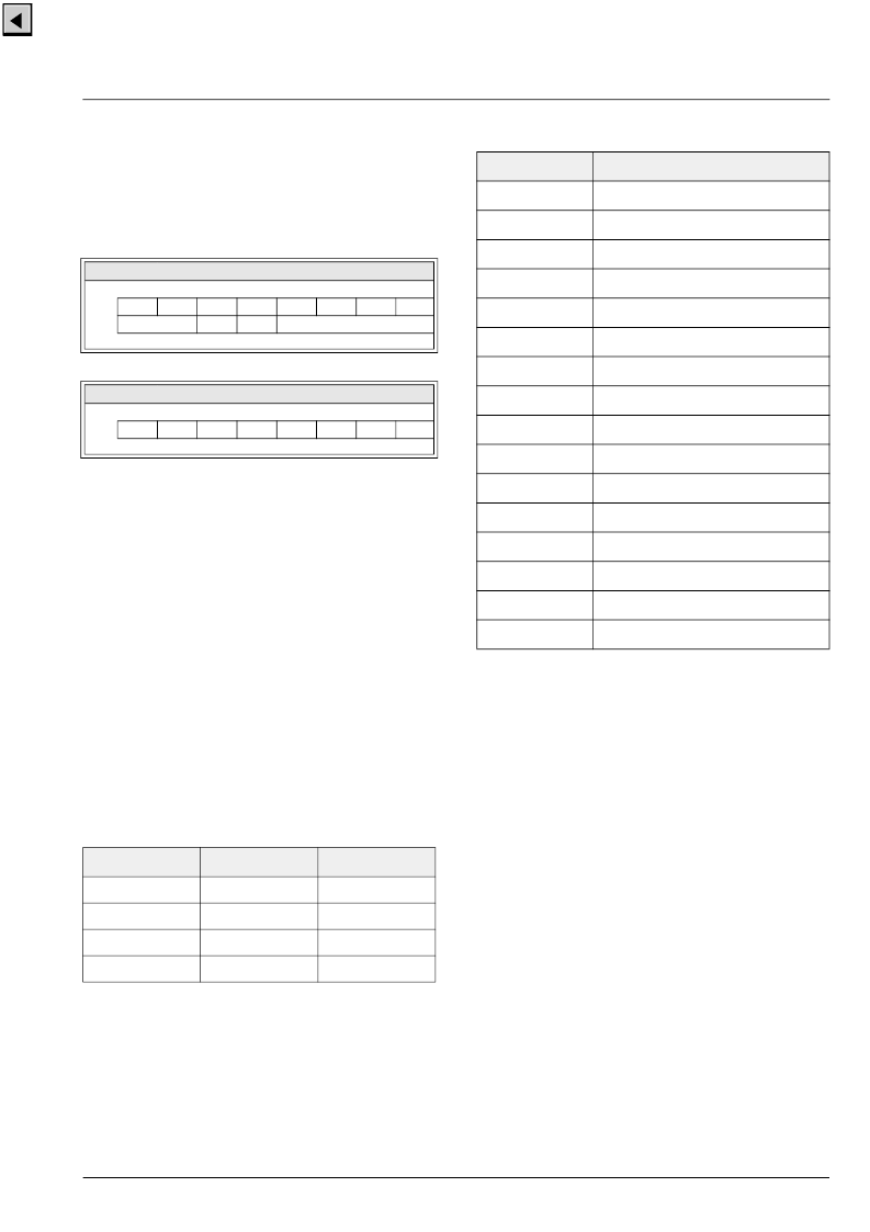
280:
1FA8
281:
AD0
282:
ADC Register 0
bit
7
6
5
4
3
2
1
0
r
EOC
CMPO
x
x
x
x
AN1
AN0
w
TSAMP
CHANNEL
reset
0
0
0
0
0
0
0
0
283:
1FA9
284:
AD1
285:
ADC Register 1
bit
7
6
5
4
3
2
1
0
r
AN9
AN8
AN7
AN6
AN5
AN4
AN3
AN2
reset
Table 5–20:
Sampling time adjustment
TSAMP
t
Sample
t
Conversion
0H
20 T
OSC
40 T
OSC
1H
60 T
OSC
80 T
OSC
2H
140 T
OSC
160 T
OSC
3H
300 T
OSC
320 T
OSC
Table 5–21:
ADC input multiplexer
CHANNEL
Port Pin
0
none
1
P10
2
P11
3
P12
4
P13
5
P14
6
P15
7
P16
8
P17
9
P20
10
P21
11
P22
12
P23
13
P24
14
P25
15
P26
相關(guān)PDF資料 |
PDF描述 |
|---|---|
| VCU2133 | High-Speed coder/decoder IC |
| VCX2150A | Surface mount 15.88 mm SQ (.625 SQ) |
| VCX2154A | Surface mount 15.88 mm SQ (.625 SQ) |
| VCXO-105N | VCXO |
| VCXO-199 | VCXO |
相關(guān)代理商/技術(shù)參數(shù) |
參數(shù)描述 |
|---|---|
| VCT3802A | 制造商:MICRONAS 制造商全稱(chēng):MICRONAS 功能描述:Video/Controller/Teletext IC Family |
| VCT3803A | 制造商:MICRONAS 制造商全稱(chēng):MICRONAS 功能描述:Video/Controller/Teletext IC Family |
| VCT3804A | 制造商:MICRONAS 制造商全稱(chēng):MICRONAS 功能描述:Video/Controller/Teletext IC Family |
| VCT3811A | 制造商:MICRONAS 制造商全稱(chēng):MICRONAS 功能描述:Video/Controller/Teletext IC Family |
| VCT3831A | 制造商:MICRONAS 制造商全稱(chēng):MICRONAS 功能描述:Video/Controller/Teletext IC Family |
發(fā)布緊急采購(gòu),3分鐘左右您將得到回復(fù)。