- 您現(xiàn)在的位置:買(mǎi)賣(mài)IC網(wǎng) > PDF目錄67592 > FUSION878A (CONEXANT SYSTEMS) COLOR SIGNAL DECODER, PQFP128 PDF資料下載
參數(shù)資料
| 型號(hào): | FUSION878A |
| 廠商: | CONEXANT SYSTEMS |
| 元件分類: | 顏色信號(hào)轉(zhuǎn)換 |
| 英文描述: | COLOR SIGNAL DECODER, PQFP128 |
| 封裝: | PLASTIC, QFP-128 |
| 文件頁(yè)數(shù): | 179/180頁(yè) |
| 文件大?。?/td> | 2067K |
| 代理商: | FUSION878A |
第1頁(yè)第2頁(yè)第3頁(yè)第4頁(yè)第5頁(yè)第6頁(yè)第7頁(yè)第8頁(yè)第9頁(yè)第10頁(yè)第11頁(yè)第12頁(yè)第13頁(yè)第14頁(yè)第15頁(yè)第16頁(yè)第17頁(yè)第18頁(yè)第19頁(yè)第20頁(yè)第21頁(yè)第22頁(yè)第23頁(yè)第24頁(yè)第25頁(yè)第26頁(yè)第27頁(yè)第28頁(yè)第29頁(yè)第30頁(yè)第31頁(yè)第32頁(yè)第33頁(yè)第34頁(yè)第35頁(yè)第36頁(yè)第37頁(yè)第38頁(yè)第39頁(yè)第40頁(yè)第41頁(yè)第42頁(yè)第43頁(yè)第44頁(yè)第45頁(yè)第46頁(yè)第47頁(yè)第48頁(yè)第49頁(yè)第50頁(yè)第51頁(yè)第52頁(yè)第53頁(yè)第54頁(yè)第55頁(yè)第56頁(yè)第57頁(yè)第58頁(yè)第59頁(yè)第60頁(yè)第61頁(yè)第62頁(yè)第63頁(yè)第64頁(yè)第65頁(yè)第66頁(yè)第67頁(yè)第68頁(yè)第69頁(yè)第70頁(yè)第71頁(yè)第72頁(yè)第73頁(yè)第74頁(yè)第75頁(yè)第76頁(yè)第77頁(yè)第78頁(yè)第79頁(yè)第80頁(yè)第81頁(yè)第82頁(yè)第83頁(yè)第84頁(yè)第85頁(yè)第86頁(yè)第87頁(yè)第88頁(yè)第89頁(yè)第90頁(yè)第91頁(yè)第92頁(yè)第93頁(yè)第94頁(yè)第95頁(yè)第96頁(yè)第97頁(yè)第98頁(yè)第99頁(yè)第100頁(yè)第101頁(yè)第102頁(yè)第103頁(yè)第104頁(yè)第105頁(yè)第106頁(yè)第107頁(yè)第108頁(yè)第109頁(yè)第110頁(yè)第111頁(yè)第112頁(yè)第113頁(yè)第114頁(yè)第115頁(yè)第116頁(yè)第117頁(yè)第118頁(yè)第119頁(yè)第120頁(yè)第121頁(yè)第122頁(yè)第123頁(yè)第124頁(yè)第125頁(yè)第126頁(yè)第127頁(yè)第128頁(yè)第129頁(yè)第130頁(yè)第131頁(yè)第132頁(yè)第133頁(yè)第134頁(yè)第135頁(yè)第136頁(yè)第137頁(yè)第138頁(yè)第139頁(yè)第140頁(yè)第141頁(yè)第142頁(yè)第143頁(yè)第144頁(yè)第145頁(yè)第146頁(yè)第147頁(yè)第148頁(yè)第149頁(yè)第150頁(yè)第151頁(yè)第152頁(yè)第153頁(yè)第154頁(yè)第155頁(yè)第156頁(yè)第157頁(yè)第158頁(yè)第159頁(yè)第160頁(yè)第161頁(yè)第162頁(yè)第163頁(yè)第164頁(yè)第165頁(yè)第166頁(yè)第167頁(yè)第168頁(yè)第169頁(yè)第170頁(yè)第171頁(yè)第172頁(yè)第173頁(yè)第174頁(yè)第175頁(yè)第176頁(yè)第177頁(yè)第178頁(yè)當(dāng)前第179頁(yè)第180頁(yè)
3.0 Electrical Interfaces
Fusion 878A
3.3 General Purpose I/O Port
PCI Video Decoder
3-14
Conexant
100600B
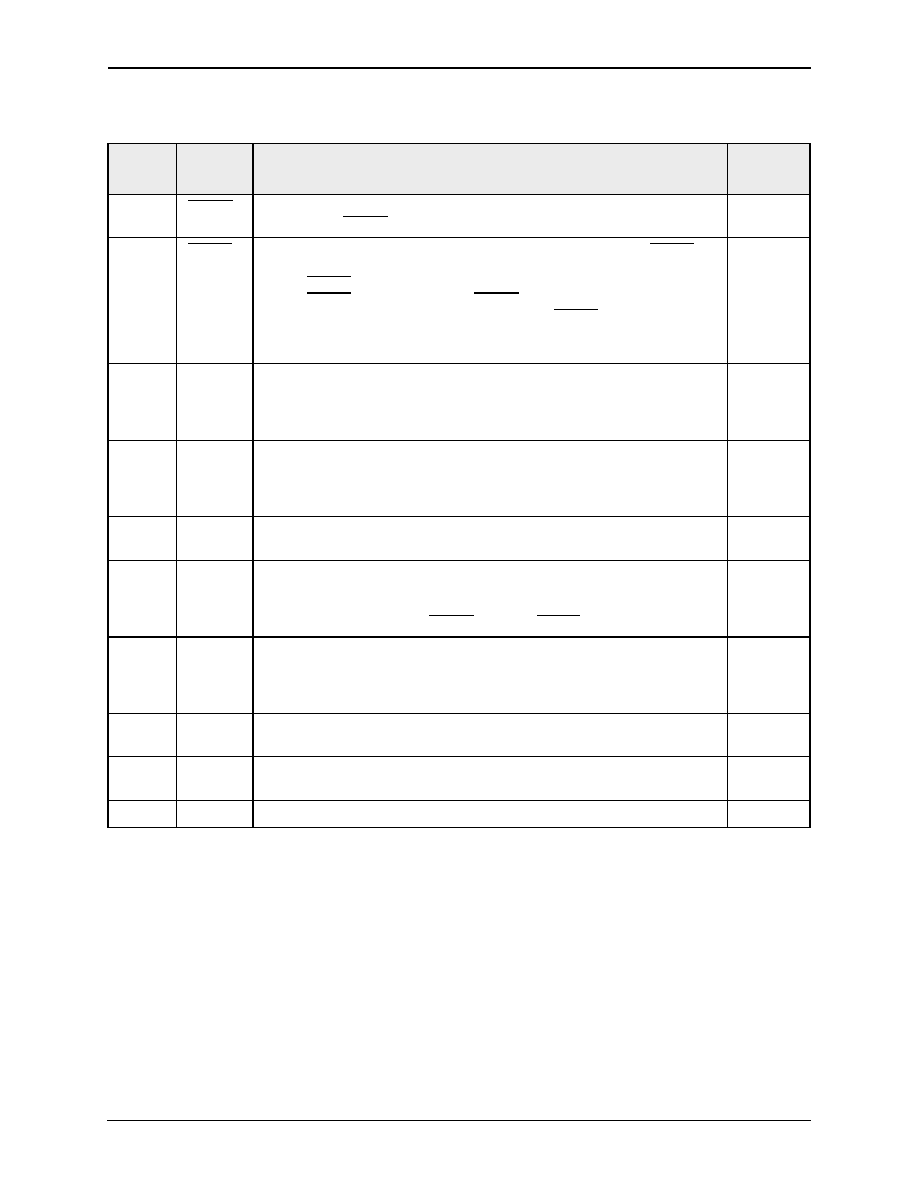
Figure 3-10 illustrates SPI output clock-data timing information. The falling
edge of the output GPCLK triggers the change in video data. This should allow
for ample setup and hold times for any device accepting the data.
Table 3-3. SPI GPIO Output Signals
GPIO
Signal
Description
Pin
Number
[23]
HRESET
A 64-clock-long active low pulse, output following the rising edge of CLKx1. The
falling edge of HRESET indicates the beginning of a new video line.
56
[22]
VRESET
An active low signal that is at least two lines long (for non-VCR sources, VRESET is
normally six lines long). It is output following the rising edge of CLKx1. The falling
edge of VRESET indicates the beginning of a new field of video output. The falling
edge of VRESET lags the falling edge of HRESET by two clock cycles at the start of an
odd field. At the start of even fields, the falling edge of VRESET is in the middle of a
scan line, horizontal count (HPIXEL/2)+1, on scan line 263 for NTSC and scan line
313 for PAL.
57
[21]
HACTIVE
An active high signal that indicates the beginning of the active video and is output
following the rising edge of CLKx1. The HACTIVE flag is used to indicate where
nonblanking pixels are present. The start and the end of the HACTIVE signal can be
adjusted by programming the HDELAY and HACTIVE registers.
58
[20]
DVALID
An active high pixel qualifier that indicates whether or not the associated pixel is
valid. DVALID is independent of the HACTIVE and VACTIVE signals. DVALID indicates
which pixels are valid. DVALID will toggle high outside of the active window,
indicating a valid pixel outside the programmed active region.
59
[19]
CBFLAG
An active high pulse that indicates when Cb data is being output on the chroma
stream. During invalid pixels, CBFLAG holds the value of the last valid pixel.
60
[18]
FIELD
When high, indicates that an even field (field 2) is being output; when low it indicates
that an odd field (field 1) is being output. The transition of FIELD is synchronous with
the end of active video (i.e. the trailing edge of ACTIVE). The same information can
also be derived by latching the HRESET signal with VRESET.
61
[17]
VACTIVE
An active high signal that indicates the beginning of the active video and is output
following the rising edge of CLKx1. The VACTIVE flag is used to indicate where
nonblanking pixels are present. The start and the end of the VACTIVE signal can be
adjusted by programming the VDELAY and VACTIVE registers.
67
[16]
VBISEL
An active high signal that indicates the beginning and end of the VBI. The end of
VBISEL will adjust accordingly when VDELAY is changed.
68
[15:8]
Y[7:0]
Digital pins for the luminance component of the video data stream.
72–69,
78–75
[7:0]
CrCb[7:0]
Digital pins for the chrominance component of the video data stream.
79–86
相關(guān)PDF資料 |
PDF描述 |
|---|---|
| FVXO-HC53BR-FREQ | VCXO, CLOCK, 0.75 MHz - 250 MHz, HCMOS OUTPUT |
| FVXO-HC72BR-FREQ | VCXO, CLOCK, 0.75 MHz - 180 MHz, HCMOS OUTPUT |
| FVXO-HC73B-FREQ | VCXO, CLOCK, 0.75 MHz - 250 MHz, HCMOS OUTPUT |
| FVXO-LC52BR-FREQ | VCXO, CLOCK, 0.75 MHz - 1000 MHz, LVDS OUTPUT |
| FVXO-LC72BR-FREQ | VCXO, CLOCK, 0.75 MHz - 1000 MHz, LVDS OUTPUT |
相關(guān)代理商/技術(shù)參數(shù) |
參數(shù)描述 |
|---|---|
| FUSZ03 | 制造商:Honeywell Sensing and Control 功能描述: |
| FUTURE 1AA PLUS | 制造商:Ansmann 功能描述: 制造商:ANSMANN AG 功能描述: |
| FUTURE 2AA PLUS | 制造商:Ansmann 功能描述: 制造商:ANSMANN AG 功能描述: |
| FUTURE 2C PLUS | 制造商:Ansmann 功能描述: 制造商:ANSMANN AG 功能描述: |
| FUTURE 3D PLUS | 制造商:Ansmann 功能描述: 制造商:ANSMANN AG 功能描述: |
發(fā)布緊急采購(gòu),3分鐘左右您將得到回復(fù)。