- 您現(xiàn)在的位置:買賣IC網(wǎng) > PDF目錄224103 > K4B4G0846B-MCF80 512M X 8 DDR DRAM, 0.3 ns, PBGA78 PDF資料下載
參數(shù)資料
| 型號: | K4B4G0846B-MCF80 |
| 元件分類: | DRAM |
| 英文描述: | 512M X 8 DDR DRAM, 0.3 ns, PBGA78 |
| 封裝: | HALOGEN FREE AND ROHS COMPLIANT, FBGA-78 |
| 文件頁數(shù): | 32/59頁 |
| 文件大小: | 1079K |
| 代理商: | K4B4G0846B-MCF80 |
第1頁第2頁第3頁第4頁第5頁第6頁第7頁第8頁第9頁第10頁第11頁第12頁第13頁第14頁第15頁第16頁第17頁第18頁第19頁第20頁第21頁第22頁第23頁第24頁第25頁第26頁第27頁第28頁第29頁第30頁第31頁當前第32頁第33頁第34頁第35頁第36頁第37頁第38頁第39頁第40頁第41頁第42頁第43頁第44頁第45頁第46頁第47頁第48頁第49頁第50頁第51頁第52頁第53頁第54頁第55頁第56頁第57頁第58頁第59頁
Page 38 of 59
Rev. 1.0 March 2009
DDP 4Gb DDR3 SDRAM
K4B4G0446B
K4B4G0846B
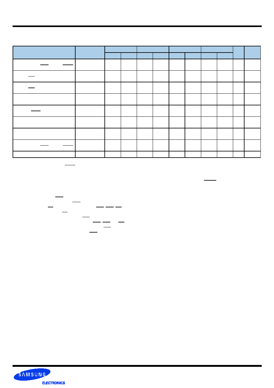
12.0 Input/Output Capacitance
[ Table 41 ] Input/Output Capacitance
Note :
1. Although the DM, TDQS and TDQS pins have different functions, the loading matches DQ and DQS
2. This parameter is not subject to production test. It is verified by design and characterization.
The capacitance is measured according to JEP147("PROCEDURE FOR MEASURING INPUT CAPACITANCE USING A VECTOR NETWORK
ANALYZER( VNA)") with VDD, VDDQ, VSS, VSSQ applied and all other pins floating (except the pin under test, CKE, RESET and ODT as necessary).
VDD=VDDQ=1.5V, VBIAS=VDD/2 and on-die termination off.
3. This parameter applies to monolithic devices only; stacked/dual-die devices are not covered here
4. Absolute value of CCK-CCK
5. Absolute value of CIO(DQS)-CIO(DQS)
6. CI applies to ODT, CS, CKE, A0-A15, BA0-BA2, RAS, CAS, WE.
7. CDI_CTRL applies to ODT, CS and CKE
8. CDI_CTRL=CI(CTRL)-0.5*(CI(CLK)+CI(CLK))
9. CDI_ADD_CMD applies to A0-A15, BA0-BA2, RAS, CAS and WE
10. CDI_ADD_CMD=CI(ADD_CMD) - 0.5*(CI(CLK)+CI(CLK))
11. CDIO=CIO(DQ,DM) - 0.5*(CIO(DQS)+CIO(DQS))
12. Maximum external load capacitance on ZQ pin: 5pF
Parameter
Symbol
DDR3-800
DDR3-1066
DDR3-1333
DDR3-1600
Units
Notes
Min
Max
Min
Max
Min
Max
Min
Max
Input/output capacitance
(DQ, DM, DQS, DQS, TDQS, TDQS)
CIO
TBD
pF
1,2,3
Input capacitance
(CK and CK)
CCK
TBD
pF
2,3
Input capacitance delta
(CK and CK)
CDCK
TBD
pF
2,3,4
Input capacitance
(All other input-only pins)
CI
TBDTBD
TBD
TBDTBD
pF
2,3,6
Input capacitance delta
(DQS and DQS)
CDDQS
TBD
pF
2,3,5
Input capacitance delta
(All control input-only pins)
CDI_CTRL
TBD
pF
2,3,7,8
Input capacitance delta
(all ADD and CMD input-onlypins)
CDI_ADD_CMD
TBD
pF
2,3,9,10
Input/output capacitance delta
(DQ, DM, DQS, DQS, TDQS, TDQS)
CDIO
TBDTBD
TBD
TBDTBD
pF
2,3,11
Input/output capacitance of ZQ pin
CZQ
TBD
pF
2, 3, 12
相關(guān)PDF資料 |
PDF描述 |
|---|---|
| K4E640411D-TC500 | 16M X 4 EDO DRAM, 50 ns, PDSO32 |
| K4F640411C-TC500 | 16M X 4 FAST PAGE DRAM, 50 ns, PDSO32 |
| K4F640412C-JC450 | 16M X 4 FAST PAGE DRAM, 45 ns, PDSO32 |
| K4T1G044QC-ZCLE6 | 256M X 4 DDR DRAM, 0.45 ns, PBGA60 |
| K4T56163QI-ZLD50 | 16M X 16 SYNCHRONOUS DRAM, 0.5 ns, PBGA84 |
相關(guān)代理商/技術(shù)參數(shù) |
參數(shù)描述 |
|---|---|
| K4B4G0846B-MCH9 | 制造商:SAMSUNG 制造商全稱:Samsung semiconductor 功能描述:DDP 4Gb B-die DDR3 SDRAM Specification |
| K4B4G0846D-BCK0000 | 制造商:Samsung Semiconductor 功能描述: |
| K4B4G1646B-HCH9000 | 制造商:Samsung Semiconductor 功能描述: |
| K4B4G1646B-HCK000 | 制造商:Samsung Semiconductor 功能描述: |
| K4B4G1646B-HCK0000 | 制造商:Samsung 功能描述:DDR SGRAM X16 TSOP2 - Trays |
發(fā)布緊急采購,3分鐘左右您將得到回復。