- 您現(xiàn)在的位置:買賣IC網(wǎng) > PDF目錄224103 > K4B4G0846B-MCF80 512M X 8 DDR DRAM, 0.3 ns, PBGA78 PDF資料下載
參數(shù)資料
| 型號(hào): | K4B4G0846B-MCF80 |
| 元件分類: | DRAM |
| 英文描述: | 512M X 8 DDR DRAM, 0.3 ns, PBGA78 |
| 封裝: | HALOGEN FREE AND ROHS COMPLIANT, FBGA-78 |
| 文件頁(yè)數(shù): | 51/59頁(yè) |
| 文件大?。?/td> | 1079K |
| 代理商: | K4B4G0846B-MCF80 |
第1頁(yè)第2頁(yè)第3頁(yè)第4頁(yè)第5頁(yè)第6頁(yè)第7頁(yè)第8頁(yè)第9頁(yè)第10頁(yè)第11頁(yè)第12頁(yè)第13頁(yè)第14頁(yè)第15頁(yè)第16頁(yè)第17頁(yè)第18頁(yè)第19頁(yè)第20頁(yè)第21頁(yè)第22頁(yè)第23頁(yè)第24頁(yè)第25頁(yè)第26頁(yè)第27頁(yè)第28頁(yè)第29頁(yè)第30頁(yè)第31頁(yè)第32頁(yè)第33頁(yè)第34頁(yè)第35頁(yè)第36頁(yè)第37頁(yè)第38頁(yè)第39頁(yè)第40頁(yè)第41頁(yè)第42頁(yè)第43頁(yè)第44頁(yè)第45頁(yè)第46頁(yè)第47頁(yè)第48頁(yè)第49頁(yè)第50頁(yè)當(dāng)前第51頁(yè)第52頁(yè)第53頁(yè)第54頁(yè)第55頁(yè)第56頁(yè)第57頁(yè)第58頁(yè)第59頁(yè)
Page 55 of 59
Rev. 1.0 March 2009
DDP 4Gb DDR3 SDRAM
K4B4G0446B
K4B4G0846B
14.4 Data Setup, Hold and Slew Rate Derating:
or all input signals the total tDS (setup time) and tDH (hold time) required is calculated by adding the data sheet tDS(base) and tDH(base) value (see
Table 52) to the
tDS and tDH (see Table 53) derating value respectively. Example: tDS (total setup time) = tDS(base) + tDS.
Setup (tDS) nominal slew rate for a rising signal is defined as the slew rate between the last crossing of VREF(DC) and the first crossing of VIH(AC)min.
Setup (tDS) nominal slew rate for a falling signal is defined as the slew rate between the last crossing of VREF(DC) and the first crossing of VIL(AC)max
(see Figure 25). If the actual signal is always earlier than the nominal slew rate line between shaded ’VREF(DC) to ac region’, use nominal slew rate for
derating value. If the actual signal is later than the nominal slew rate line anywhere
between shaded ’VREF(DC) to ac region’, the slew rate of a tangent line to the actual signal from the ac level to dc level is used for derating value (see
Figure 27).
Hold (tDH) nominal slew rate for a rising signal is defined as the slew rate between the last crossing of VIL(DC)max and the first crossing of VREF(DC).
Hold (tDH) nominal slew rate for a falling signal is defined as the slew rate between the last crossing of VIH(DC)min and the first crossing of VREF(DC)
(see Figure 26). If the actual signal is always later than the nominal slew rate line between shaded ’dc level to VREF(DC) region’, use nominal slew rate for
derating value. If the actual signal is earlier than the nominal slew rate line anywhere between shaded ’dc to VREF(DC) region’, the slew rate of a tangent
line to the actual signal from the dc level to VREF(DC) level is used for derating value (see Figure 28).
For a valid transition the input signal has to remain above/below VIH/IL(AC) for some time tVAC (see Table 54).
Although for slow slew rates the total setup time might be negative (i.e. a valid input signal will not have reached VIH/IL(AC) at the time of the rising clock
transition) a valid input signal is still required to complete the transition and reach VIH/IL(AC).
For slew rates in between the values listed in the tables the derating values may obtained by linear interpolation.
These values are typically not subject to production test. They are verified by design and characterization
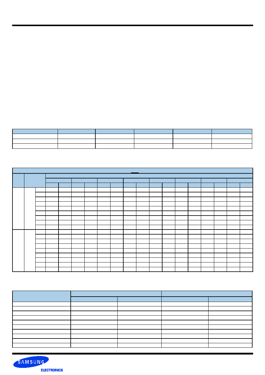
[ Table 52 ] Data Setup and Hold Base-Value
Note : AC/DC referenced for 1V/ns DQ-slew rate and 2 V/ns DQS slew rate)
[ Table 53 ] Derating values DDR3-800/1066/1333/1600 tIS/tIH-ac/dc based
Note : a. Cell contents shaded in red are defined as ’not supported’.
[ Table 54 ] Required time tVAC above VIH(AC) {blow VIL(AC)} for valid transition
[ps]
DDR3-800
DDR3-1066
DDR3-1333
DDR3-1600
reference
tDS(base)
75
25
30
10
VIH/L(AC)
tDH(base)
150
100
65
45
VIH/L(DC)
tDS(AC150)
75+50
25+50
-
-VIH/L(AC)
tDS, tDH Derating [ps] AC/DC baseda
DQS,DQS Differential Slew Rate
4.0 V/ns
3.0 V/ns
2.0 V/ns
1.8 V/ns
1.6 V/ns
1.4V/ns
1.2V/ns
1.0V/ns
tDS
tDH
tDS
tDH
tDS
tDH
tDS
tDH
tDS
tDH
tDS
tDH
tDS
tDH
tDS
tDH
DDR3
-
800/
1066
DQ
Slew
rate
V/ns
2.0
88
50
88
50
88
50
-
---
--
-
1.5
5934
6742
-
1.0
0
00
08
8
16
-
0.9
-
-2-4
6
4
14
12
22
20
-
0.8
-
-6
-10
2
-2
10
6
18
14
26
24
-
0.7
-
-3
-8
5
0
13
8
21
18
29
34
0.6
-
-1
-10
7
-2
15
8
23
24
0.5
-
--
-
-11
-16
-2
-6
6
10
0.4
-
--
-
-30
-26
-22
-10
DDR3
-
1333/
1600
DQ
Slew
rate
V/ns
2.0
75
50
75
50
75
50
-
---
--
-
1.5
5034
5842
-
1.0
0
00
08
8
16
-
0.9
-
0
-4
0
-4
8
4
1612
2420
-
0.8
-
0
-10
8
-2
16
6
24
14
32
24
-
0.7
-
8
-8
16
0
24
8
32
18
40
34
0.6
-
15
-10
23
-2
31
8
39
24
0.5
-
14
-16
22
-6
30
10
0.4
-
--
-
7
-26
15
-10
Slew Rate[V/ns]
tVAC[ps] DDR3-800/1066
tVAC[ps] DDR3-1333/1600
min
max
min
max
>2.0
75
-
175
-
2.0
57
-
170
-
1.5
50
-
167
-
1.0
38
-
163
-
0.9
34
-
162
-
0.8
29
-
161
-
0.7
22
-
159
-
0.6
13
-
155
-
0.5
0
-
155
-
<0.5
0
-
150
-
相關(guān)PDF資料 |
PDF描述 |
|---|---|
| K4E640411D-TC500 | 16M X 4 EDO DRAM, 50 ns, PDSO32 |
| K4F640411C-TC500 | 16M X 4 FAST PAGE DRAM, 50 ns, PDSO32 |
| K4F640412C-JC450 | 16M X 4 FAST PAGE DRAM, 45 ns, PDSO32 |
| K4T1G044QC-ZCLE6 | 256M X 4 DDR DRAM, 0.45 ns, PBGA60 |
| K4T56163QI-ZLD50 | 16M X 16 SYNCHRONOUS DRAM, 0.5 ns, PBGA84 |
相關(guān)代理商/技術(shù)參數(shù) |
參數(shù)描述 |
|---|---|
| K4B4G0846B-MCH9 | 制造商:SAMSUNG 制造商全稱:Samsung semiconductor 功能描述:DDP 4Gb B-die DDR3 SDRAM Specification |
| K4B4G0846D-BCK0000 | 制造商:Samsung Semiconductor 功能描述: |
| K4B4G1646B-HCH9000 | 制造商:Samsung Semiconductor 功能描述: |
| K4B4G1646B-HCK000 | 制造商:Samsung Semiconductor 功能描述: |
| K4B4G1646B-HCK0000 | 制造商:Samsung 功能描述:DDR SGRAM X16 TSOP2 - Trays |
發(fā)布緊急采購(gòu),3分鐘左右您將得到回復(fù)。