- 您現(xiàn)在的位置:買賣IC網(wǎng) > PDF目錄359412 > VPX3224D (Electronic Theatre Controls, Inc.) Video Pixel Decoders PDF資料下載
參數(shù)資料
| 型號(hào): | VPX3224D |
| 廠商: | Electronic Theatre Controls, Inc. |
| 英文描述: | Video Pixel Decoders |
| 中文描述: | 視頻解碼器像素 |
| 文件頁數(shù): | 36/92頁 |
| 文件大小: | 672K |
| 代理商: | VPX3224D |
第1頁第2頁第3頁第4頁第5頁第6頁第7頁第8頁第9頁第10頁第11頁第12頁第13頁第14頁第15頁第16頁第17頁第18頁第19頁第20頁第21頁第22頁第23頁第24頁第25頁第26頁第27頁第28頁第29頁第30頁第31頁第32頁第33頁第34頁第35頁當(dāng)前第36頁第37頁第38頁第39頁第40頁第41頁第42頁第43頁第44頁第45頁第46頁第47頁第48頁第49頁第50頁第51頁第52頁第53頁第54頁第55頁第56頁第57頁第58頁第59頁第60頁第61頁第62頁第63頁第64頁第65頁第66頁第67頁第68頁第69頁第70頁第71頁第72頁第73頁第74頁第75頁第76頁第77頁第78頁第79頁第80頁第81頁第82頁第83頁第84頁第85頁第86頁第87頁第88頁第89頁第90頁第91頁第92頁
PRELIMINARY DATA SHEET
VPX 3225D, VPX 3224D
36
Micronas
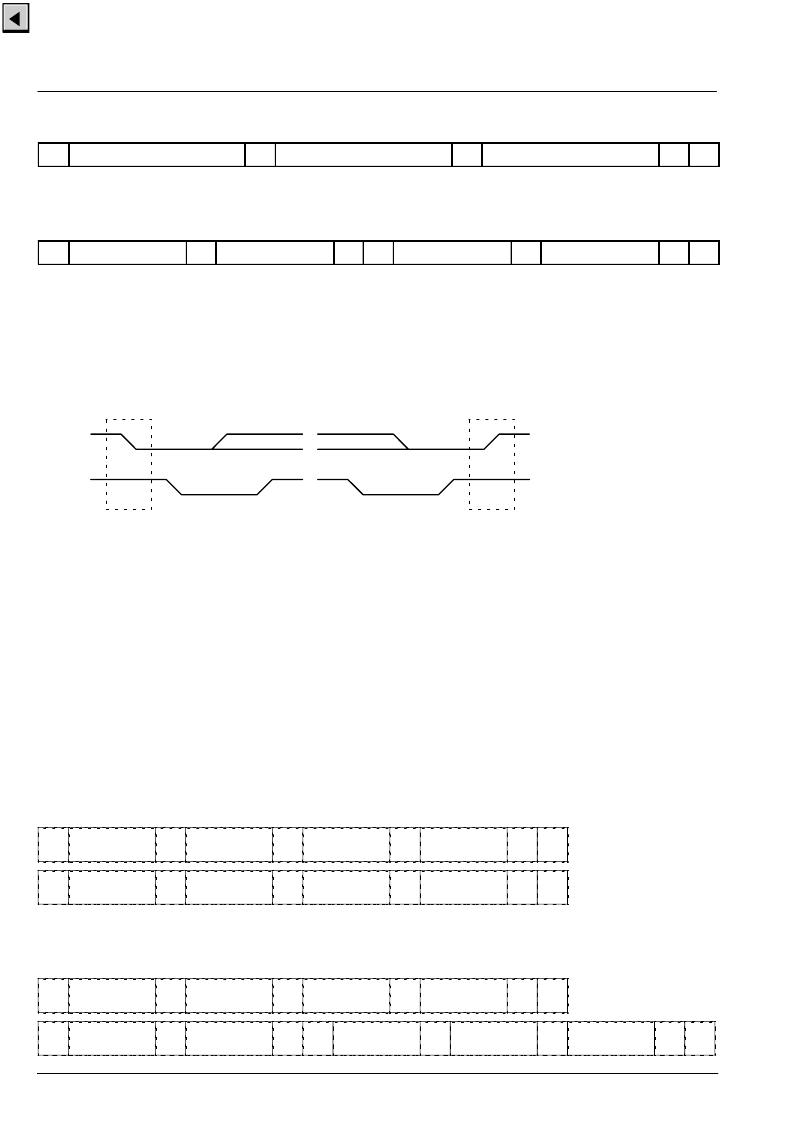
Write to Hardware Control Registers
S
1 0 0 0 0 1 1 0
ACK
sub-addr
ACK
send data-byte
ACK
P
Read from Hardware Control Registers
S
1 0 0 0 0 1 1 0
ACK
sub-addr
ACK
S
1 0 0 0 0 1 1 1
ACK
receive data-byte
NAK
P
Note:
S =
P =
ACK = Acknowledge-Bit (active low on SDA from receiving device)
NAK = No Acknowledge-Bit (inactive high on SDA from receiving device)
I
2
C-Bus Start Condition
I
2
C-Bus Stop Condition
Fig. 2–40:
I
2
C bus protocol
(MSB first)
SDA
SCL
1
0
S
P
2.14.5. FP Control and Status Registers
Due to the internal architecture of the VPX, the IC cannot
react immediately to all I
2
C requests which interact with
the embedded processor (FP). The maximum response
timing is appr. 20 ms (one TV field) for the FP processor
if TV standard switching is active. If the addressed pro-
cessor is not ready for further transmissions on the I
2
C
bus, the clock line SCL is pulled low. This puts the cur-
rent transmission into a wait state called clock synchro-
nization. After a certain period of time, the VPX releases
the clock and the interrupted transmission is carried on.
Before accessing the address or data registers for the
FP interface (FPRD, FPWR, FPDAT), make sure that
the busy bit of FP is cleared (FPSTA).
Write to FP
S
1 0 0 0 0 1 1 0
ACK
FPWR
ACK
send FP-address-
byte high
ACK
send FP-address-
byte low
ACK
P
S
1 0 0 0 0 1 1 0
ACK
FPDAT
ACK
send data-byte
high
ACK
send data-byte
low
ACK
P
Read from FP
S
1 0 0 0 0 1 1 0
ACK
FPRD
ACK
send FP-address-
byte high
ACK
send FP-address-
byte low
ACK
P
S
1 0 0 0 0 1 1 0
ACK
FPDAT
ACK
S
1 0 0 0 0 1 1 1
ACK
receive data-byte
high
ACK
receive data-byte
low
NAK
P
相關(guān)PDF資料 |
PDF描述 |
|---|---|
| VPX3224E | Video Pixel Decoders |
| VPX322XE | Video Pixel Decoders |
| VQ1000J | N-Channel Enhancement-Mode MOSFET Transistor(最小漏源擊穿電壓60V,夾斷電流0.225A的N溝道增強(qiáng)型MOSFET晶體管) |
| VQ1000J | N-Channel 60-V (D-S) MOSFET |
| VQ1001J | Dual N-Channel 30-V (D-S) MOSFET with Schottky Diode |
相關(guān)代理商/技術(shù)參數(shù) |
參數(shù)描述 |
|---|---|
| VPX3224D-C3 | 制造商:未知廠家 制造商全稱:未知廠家 功能描述:Microprocessor |
| VPX3224E | 制造商:MICRONAS 制造商全稱:MICRONAS 功能描述:Video Pixel Decoders |
| VPX3225D | 制造商:未知廠家 制造商全稱:未知廠家 功能描述:Video Pixel Decoders |
| VPX3225D-C3 | 制造商:未知廠家 制造商全稱:未知廠家 功能描述:Microprocessor |
| VPX3225E | 制造商:MICRONAS 制造商全稱:MICRONAS 功能描述:Video Pixel Decoders |
發(fā)布緊急采購,3分鐘左右您將得到回復(fù)。