- 您現(xiàn)在的位置:買賣IC網(wǎng) > PDF目錄359412 > VPX3224D (Electronic Theatre Controls, Inc.) Video Pixel Decoders PDF資料下載
參數(shù)資料
| 型號(hào): | VPX3224D |
| 廠商: | Electronic Theatre Controls, Inc. |
| 英文描述: | Video Pixel Decoders |
| 中文描述: | 視頻解碼器像素 |
| 文件頁數(shù): | 44/92頁 |
| 文件大小: | 672K |
| 代理商: | VPX3224D |
第1頁第2頁第3頁第4頁第5頁第6頁第7頁第8頁第9頁第10頁第11頁第12頁第13頁第14頁第15頁第16頁第17頁第18頁第19頁第20頁第21頁第22頁第23頁第24頁第25頁第26頁第27頁第28頁第29頁第30頁第31頁第32頁第33頁第34頁第35頁第36頁第37頁第38頁第39頁第40頁第41頁第42頁第43頁當(dāng)前第44頁第45頁第46頁第47頁第48頁第49頁第50頁第51頁第52頁第53頁第54頁第55頁第56頁第57頁第58頁第59頁第60頁第61頁第62頁第63頁第64頁第65頁第66頁第67頁第68頁第69頁第70頁第71頁第72頁第73頁第74頁第75頁第76頁第77頁第78頁第79頁第80頁第81頁第82頁第83頁第84頁第85頁第86頁第87頁第88頁第89頁第90頁第91頁第92頁
PRELIMINARY DATA SHEET
VPX 3225D, VPX 3224D
44
Micronas
2.17. Enable/Disable of Output Signals
In order to enable the output pins of the VPX to achieve
the high impedance/tristate mode, various controls have
been implemented. The following paragraphs give an
overview of the different tristate modes of the output sig-
nals. It is valid for all output pins, except the XTAL2
(which is the oscillator output) and the VRT pin (which is
an analog reference voltage).
BS (Boundary Scan) Mode:
The tristate control by the test access port TAP for
boundary scan has the highest priority. Even if the TAP-
controller is in the EXTEST or CLAMP mode, the tristate
behavior is only defined by the state of the different
boundary scan registers for enable control. If the TAP
controller is in HIGHZ mode, then all output pins are in
tristate mode independently of the state of the different
boundary scan registers for enable control.
RESET State:
If the TAP-controller is not in the EXTEST mode, then the
RESET-state defines the state of all digital outputs. The
only exception is made for the data output of the bound-
ary scan interface TDO. If the circuit is in reset condition
(RES = 0), then all output interfaces are in tristate mode.
I
2
C Control:
The tristate condition of groups of signals can also be
controlled by setting the I
2
C-Register 0xF2. If the circuit
is neither in EXTEST mode nor RESET state, then the
I
2
C-Register 0xF2 defines whether the output is in tris-
tate condition or not (see “I
2
C-Registers VPX Back-
end”).
Output Enable Input OE:
The output enable signal OE only effects the video out-
put ports. If the previous three conditions do not cause
the output drivers to go into high impedance mode, then
the OE signal defines the driving conditions of the video
data ports.
The OE pin function can be disabled via I
2
C register
0xF2 [oeq_dis]. The OE signal will either directly con-
nect the output drivers or it will be latched internally with
the LLC signal depending on I
2
C register 0xF2 [latoeq].
Additionally, a delay of 1 LLC clock cycle can be enabled
with I
2
C register 0xF2 [oeqdel].
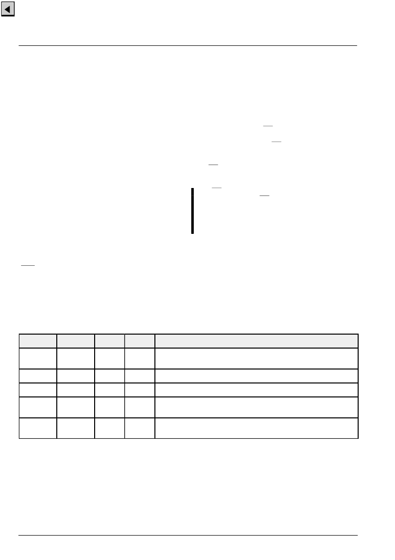
Table 2–17:
Output driver configuration
EXTEST
RESET
I
2
C
OE#
Driver Stages
active
–
–
–
Output driver stages are defined by the state of the different
boundary scan enable registers.
inactive
active
–
–
Output drivers are in high impedance mode.
inactive
inactive
= 0
–
Output drivers are in high impedance mode. PIXCLK is working.
inactive
inactive
= 1
= 0
Output drivers HREF, VREF, FIELD, VACT, LLC, are working.
Outputs A[7:0] and B[7:0] are working
inactive
inactive
= 1
= 1
Output drivers HREF, VREF, FIELD, VACT, LLC, are working.
Output drivers of A[7:0] and B[7:0] are in high impedance mode.
Remark:
EXTEST mode is an instruction conforming to the standard for Boundary Scan Test IEEE 1149.1 – 1990
相關(guān)PDF資料 |
PDF描述 |
|---|---|
| VPX3224E | Video Pixel Decoders |
| VPX322XE | Video Pixel Decoders |
| VQ1000J | N-Channel Enhancement-Mode MOSFET Transistor(最小漏源擊穿電壓60V,夾斷電流0.225A的N溝道增強(qiáng)型MOSFET晶體管) |
| VQ1000J | N-Channel 60-V (D-S) MOSFET |
| VQ1001J | Dual N-Channel 30-V (D-S) MOSFET with Schottky Diode |
相關(guān)代理商/技術(shù)參數(shù) |
參數(shù)描述 |
|---|---|
| VPX3224D-C3 | 制造商:未知廠家 制造商全稱:未知廠家 功能描述:Microprocessor |
| VPX3224E | 制造商:MICRONAS 制造商全稱:MICRONAS 功能描述:Video Pixel Decoders |
| VPX3225D | 制造商:未知廠家 制造商全稱:未知廠家 功能描述:Video Pixel Decoders |
| VPX3225D-C3 | 制造商:未知廠家 制造商全稱:未知廠家 功能描述:Microprocessor |
| VPX3225E | 制造商:MICRONAS 制造商全稱:MICRONAS 功能描述:Video Pixel Decoders |
發(fā)布緊急采購,3分鐘左右您將得到回復(fù)。