- 您現(xiàn)在的位置:買賣IC網(wǎng) > PDF目錄359438 > VT6516 (Electronic Theatre Controls, Inc.) 16/12 PORT 10/1000 ASE T/TX PDF資料下載
參數(shù)資料
| 型號(hào): | VT6516 |
| 廠商: | Electronic Theatre Controls, Inc. |
| 英文描述: | 16/12 PORT 10/1000 ASE T/TX |
| 中文描述: | 16/12港口10/1000日月光噸/德克薩斯州 |
| 文件頁數(shù): | 22/73頁 |
| 文件大?。?/td> | 440K |
| 代理商: | VT6516 |
第1頁第2頁第3頁第4頁第5頁第6頁第7頁第8頁第9頁第10頁第11頁第12頁第13頁第14頁第15頁第16頁第17頁第18頁第19頁第20頁第21頁當(dāng)前第22頁第23頁第24頁第25頁第26頁第27頁第28頁第29頁第30頁第31頁第32頁第33頁第34頁第35頁第36頁第37頁第38頁第39頁第40頁第41頁第42頁第43頁第44頁第45頁第46頁第47頁第48頁第49頁第50頁第51頁第52頁第53頁第54頁第55頁第56頁第57頁第58頁第59頁第60頁第61頁第62頁第63頁第64頁第65頁第66頁第67頁第68頁第69頁第70頁第71頁第72頁第73頁
VIA Technologies, Inc.
Preliminary VT6516 Datarsheet
-
22-
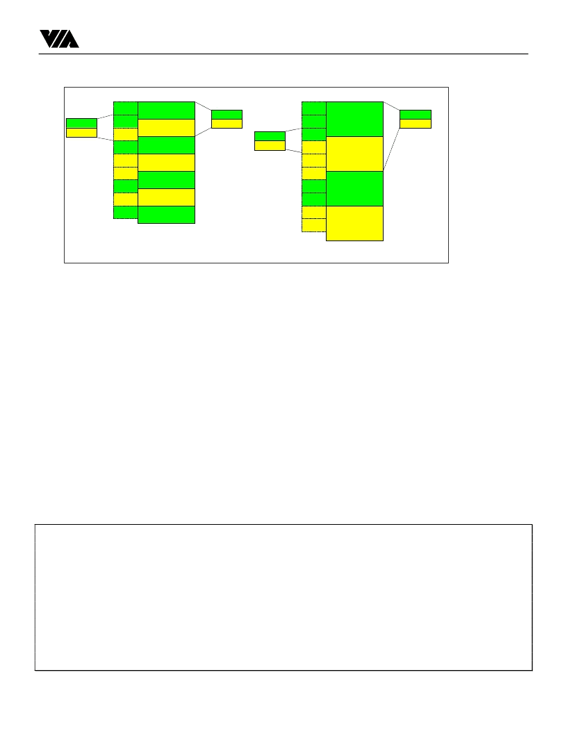
Figure 3-3
Following as the listing and figure 3-6 is the algorithm of initialization procedures for 2 bank free list of
SDRAM.
For 16 Mbit SDRAM as following,
-- Bank0 free link list:
128, 129, 131, 134, 136, 137, 139, 142, 144, 145, 147, 150, 152, 153, 155, 158, 160,...
-- Bank1 free link list:
130, 132, 133, 135, 138, 140, 141, 143, 146, 148, 149, 151, 154, 156, 157, 159, 162, 164, ...
For 64 Mbit SDRAM as following,
-- Bank0 free link list:
128 , 129 , 130 , 134 , 135 , 139 , 140 , 141 , 144 , 145 , 146 , 150 , 151 , 155 , 156 , 157 , 160 , ...
--Bank1 free link list:
131 , 132 , 133 , 136 , 137 , 138 , 142 , 143 , 147 , 148 , 149 , 152 , 153 , 154 , 158 , 159 , 163 , …
Figure 3-6: Algorithm of Initialization of Free Link Lists.
#define SRAM_ADDR_REG0 0x2001
#define SRAM_ADDR_REG1 0x2002
#define SRAM_ADDR_REG2 0x2003
#define SRAM_DATA_REG0 0x2004
#define SRAM_DATA_REG1 0x2005
#define SRAM_DATA_REG2 0x2006
#define SRAM_DATA_REG3 0x2007
#define SRAM_CMD_REG 0x2008
#define SRAM_STATUS_REG 0x2009
#define SRAM_ACCESS_IDLE 0x01
#define NULL_PTR 0x7FFFF
void writeLinkEntry(int entryID, int nextID)
{
reg_byte_write (SRAM_ADDR_REG0, entryID*3 & 0x0FF);
reg_byte_cont_write (((entryID*3) >> 8) & 0x0FF);
reg_byte_cont_write (((entryID*3) >> 16) & 0x0FF);
2K
2K
2K
2K
128/0
129/0
130/1
131/0
132/1
Bank 0
Bank 1
2K
133/1
2K
2K
134/0
135/1
136/0
Link/
Frame
Memory Bank
List 0
List 1
4K
4K
128/0
129/0
131/1
130/0
132/1
Bank 0
Bank 1
133/1
134/0
136/1
135/0
Links/
List
Memory Bank
List 0
List 1
4K
4K
137/1
16MBits SDRAM
64MBits SDRAM
相關(guān)PDF資料 |
PDF描述 |
|---|---|
| VT70A144 | |
| VT74A451 | |
| VT74A901 | |
| VT77A142 | |
| VT77A202 | |
相關(guān)代理商/技術(shù)參數(shù) |
參數(shù)描述 |
|---|---|
| VT-6-6 | 制造商:Panduit Corp 功能描述:BOLT TERM 70MM 57MM - Bulk 制造商:Panduit Corp 功能描述:Bolt Terminal 70mm 57mm |
| VT6J1 | 制造商:ROHM 制造商全稱:Rohm 功能描述:1.2V Drive Pch + Pch MOSFET |
| VT6K1 | 制造商:ROHM 制造商全稱:Rohm 功能描述:1.2V Drive Nch + Nch MOSFET |
| VT6K1T2CR | 制造商:ROHM Semiconductor 功能描述: |
| VT6M1 | 制造商:ROHM 制造商全稱:Rohm 功能描述:1.2V Drive Nch + Pch MOSFET |
發(fā)布緊急采購,3分鐘左右您將得到回復(fù)。