- 您現(xiàn)在的位置:買賣IC網(wǎng) > PDF目錄366550 > AM79C974 (Advanced Micro Devices, Inc.) PCnetTM-SCSI Combination Ethernet and SCSI Controller for PCI Systems PDF資料下載
參數(shù)資料
| 型號: | AM79C974 |
| 廠商: | Advanced Micro Devices, Inc. |
| 英文描述: | PCnetTM-SCSI Combination Ethernet and SCSI Controller for PCI Systems |
| 中文描述: | PCnetTM -的SCSI結(jié)合以太網(wǎng)和SCSI控制器PCI系統(tǒng) |
| 文件頁數(shù): | 54/153頁 |
| 文件大?。?/td> | 838K |
| 代理商: | AM79C974 |
第1頁第2頁第3頁第4頁第5頁第6頁第7頁第8頁第9頁第10頁第11頁第12頁第13頁第14頁第15頁第16頁第17頁第18頁第19頁第20頁第21頁第22頁第23頁第24頁第25頁第26頁第27頁第28頁第29頁第30頁第31頁第32頁第33頁第34頁第35頁第36頁第37頁第38頁第39頁第40頁第41頁第42頁第43頁第44頁第45頁第46頁第47頁第48頁第49頁第50頁第51頁第52頁第53頁當(dāng)前第54頁第55頁第56頁第57頁第58頁第59頁第60頁第61頁第62頁第63頁第64頁第65頁第66頁第67頁第68頁第69頁第70頁第71頁第72頁第73頁第74頁第75頁第76頁第77頁第78頁第79頁第80頁第81頁第82頁第83頁第84頁第85頁第86頁第87頁第88頁第89頁第90頁第91頁第92頁第93頁第94頁第95頁第96頁第97頁第98頁第99頁第100頁第101頁第102頁第103頁第104頁第105頁第106頁第107頁第108頁第109頁第110頁第111頁第112頁第113頁第114頁第115頁第116頁第117頁第118頁第119頁第120頁第121頁第122頁第123頁第124頁第125頁第126頁第127頁第128頁第129頁第130頁第131頁第132頁第133頁第134頁第135頁第136頁第137頁第138頁第139頁第140頁第141頁第142頁第143頁第144頁第145頁第146頁第147頁第148頁第149頁第150頁第151頁第152頁第153頁
AMD
P R E L I M I N A R Y
54
Am79C974
the controller portion of the Am79C974 controller sees
the first ISRDCLK transition. This also strobes in the in-
coming fifth bit to the MENDEC as Manchester “1”.
IRXDAT may make a transition after the ISRDCLK rising
edge in bit cell 5, but its state is still undefined. The
Manchester “1” at bit 5 is clocked to IRXDAT output at
1/4 bit time in bit cell 6.
PLL Tracking
After clock acquisition, the phase-locked clock is com-
pared to the incoming transition at the bit cell center
(BCC) and the resulting phase error is applied to a cor-
rection circuit. This circuit ensures that the phase-
locked clock remains locked on the received signal.
Individual bit cell phase corrections of the Voltage Con-
trolled Oscillator (VCO) are limited to 10% of the phase
difference between BCC and phase-locked clock.
Hence, input data jitter is reduced in ISRDCLK by
10to1.
Carrier Tracking and End of Message
The carrier detection circuit monitors the DI
±
inputs after
IRXCRS is asserted for an end of message. IRXCRS
de-asserts 1 to 2 bit times after the last positive transi-
tion on the incoming message. This initiates the end of
reception cycle. The time delay from the last rising edge
of the message to IRXCRS de-assert allows the last bit
to be strobed by ISRDCLK and transferred to the con-
troller section, but prevents any extra bit(s) at the end
ofmessage.
Data Decoding
The data receiver is a comparator with clocked output to
minimize noise sensitivity to the DI
±
inputs. Input error is
less than
±
35 mV to minimize sensitivity to input rise and
fall time. ISRDCLK strobes the data receiver output at
1/4 bit time to determine the value of the Manchester bit,
and clocks the data out on IRXDAT on the following
ISRDCLK. The data receiver also generates the signal
used for phase detector comparison to the internal
MENDEC voltage controlled oscillator (VCO).
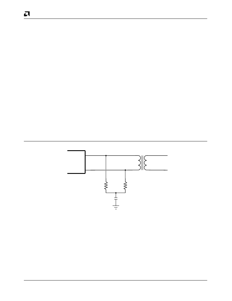
Differential Input Terminations
The differential input for the Manchester data (DI
±
)
should be externally terminated by two 40.2
±
1% re-
sistors and one optional common-mode bypass capaci-
tor, as shown in the Differential Input Termination
diagram below. The differential input impedance, Z
IDF
,
and the common-mode input impedance, Z
ICM
, are
specified so that the Ethernet specification for cable ter-
mination impedance is met using standard 1% resistor
terminators. If SIP devices are used, 39
is the nearest
usable value. The CI
±
differential inputs are terminated
in exactly the same way as the DI
±
pair.
18681A-24
Am79C974
DI+
DI-
40.2
40.2
0.01
μ
F
to
0.1
μ
F
AUI Isolation
Transformer
Figure 20.
Differential Input Termination
相關(guān)PDF資料 |
PDF描述 |
|---|---|
| AM79C974KCW | PCnetTM-SCSI Combination Ethernet and SCSI Controller for PCI Systems |
| AM79C975 | PCnet⑩-FAST III Single-Chip 10/100 Mbps PCI Ethernet Controller with Integrated PHY |
| AM79C973 | PCnet⑩-FAST III Single-Chip 10/100 Mbps PCI Ethernet Controller with Integrated PHY |
| AM79C973KCW | PCnet⑩-FAST III Single-Chip 10/100 Mbps PCI Ethernet Controller with Integrated PHY |
| AM79C975KCW | PCnet⑩-FAST III Single-Chip 10/100 Mbps PCI Ethernet Controller with Integrated PHY |
相關(guān)代理商/技術(shù)參數(shù) |
參數(shù)描述 |
|---|---|
| AM79C974KC | 制造商:Advanced Micro Devices 功能描述: |
| AM79C974KC/W | 制造商:未知廠家 制造商全稱:未知廠家 功能描述:LAN Node Controller |
| AM79C974KCW | 制造商:AMD 制造商全稱:Advanced Micro Devices 功能描述:PCnetTM-SCSI Combination Ethernet and SCSI Controller for PCI Systems |
| AM79C975 | 制造商:AMD 制造商全稱:Advanced Micro Devices 功能描述:PCnet⑩-FAST III Single-Chip 10/100 Mbps PCI Ethernet Controller with Integrated PHY |
發(fā)布緊急采購,3分鐘左右您將得到回復(fù)。