- 您現(xiàn)在的位置:買(mǎi)賣(mài)IC網(wǎng) > PDF目錄370702 > HSP3824VI (Harris Corporation) Direct Sequence Spread Spectrum Baseband Processor PDF資料下載
參數(shù)資料
| 型號(hào): | HSP3824VI |
| 廠商: | Harris Corporation |
| 元件分類: | 基帶處理器 |
| 英文描述: | Direct Sequence Spread Spectrum Baseband Processor |
| 中文描述: | 直接序列擴(kuò)頻基帶處理器 |
| 文件頁(yè)數(shù): | 12/41頁(yè) |
| 文件大小: | 276K |
| 代理商: | HSP3824VI |
第1頁(yè)第2頁(yè)第3頁(yè)第4頁(yè)第5頁(yè)第6頁(yè)第7頁(yè)第8頁(yè)第9頁(yè)第10頁(yè)第11頁(yè)當(dāng)前第12頁(yè)第13頁(yè)第14頁(yè)第15頁(yè)第16頁(yè)第17頁(yè)第18頁(yè)第19頁(yè)第20頁(yè)第21頁(yè)第22頁(yè)第23頁(yè)第24頁(yè)第25頁(yè)第26頁(yè)第27頁(yè)第28頁(yè)第29頁(yè)第30頁(yè)第31頁(yè)第32頁(yè)第33頁(yè)第34頁(yè)第35頁(yè)第36頁(yè)第37頁(yè)第38頁(yè)第39頁(yè)第40頁(yè)第41頁(yè)

12
HSP3824
The procedure for setting the ADC references to accommo-
date various input signal voltage levels is to set the reference
voltages so that the ADC calibration circuit is operating at
half scale. This leaves the maximum amount of adjustment
room for circuit tolerances.
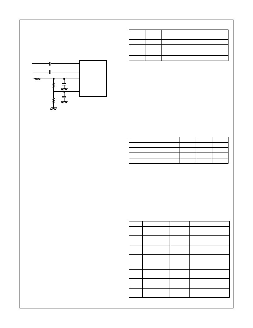
Figure 8 illustrates the suggested interface configuration for
the ADCs and the reference circuits.
FIGURE 8. INTERFACES
ADC Calibration Circuit and Registers
The ADC compensation or calibration circuit is designed to
optimize ADC performance for the I and Q inputs by main-
taining the full 3-bit resolution of the outputs. There are two
registers (CR 11 AD_CAL_POS and CR 12 AD_CAL_NEG)
that set the parameters for the internal I and Q ADC calibra-
tion circuit.
Both I and Q ADC outputs are monitored by the ADC calibra-
tion circuit and if either has a full scale value, a 24-bit accu-
mulator
is
incremented
as
AD_CAL_POS. If neither has a full scale value, the accumu-
lator
is
decremented
as
AD_CAL_NEG.
defined
by
parameter
defined
by
parameter
A loop gain reduction is accomplished by using only the 5
MSBs out of the 24 bits to drive a D/A converter that adjusts
the ADCs reference. The compensation adjustment is
updated at 2kHz rate for a 2 MBPS operation. The ADC cali-
bration circuit is only intended to remove slow component
variations.
The ratio of the values from the two registers CR11 and
CR12 set the probability that either the I or Q ADC converter
will be at the saturation. The probability is set by
(AD_CAL_POS)/(AD_CAL_NEG).
This also sets the levels so that operation with either NOISE
or DPSK is approximately the same. It is assumed that the
RF and IF sections of the receiver have enough gain to
cause limiting on thermal noise. This will keep the levels at
the ADC approximately same regardless of whether signal is
present or not.
The ADC calibration voltage is automatically held during
transmit in half duplex operation.
The ADC calibration circuit operation can be defined through
CR 1, bits 1 and 0. Table 3 illustrates the possible
configurations.
0.01
μ
F
0.01
μ
F
3.9K
8.2K
9.1K
I
Q
2V
I
IN
Q
IN
V
REFP
V
REFN
HSP3824
0.01
μ
F
0.01
μ
F
RSSI ADC Interface
The Receive Signal Strength Indication (RSSI) analog signal is
input to a 6-bit ADC, indicating 64 discrete levels of received
signal strength. This ADC measures a DC voltage, so its input
must be DC coupled. Pin 16 (V
REFP
) sets the reference for the
RSSI ADC converter. V
REFP
is common for the I and Q and
RSSI ADCs. The RSSI signal is used as an input to the pro-
grammable Clear Channel Assessment algorithm of the
HSP3824. The RSSI ADC output is stored in an 8-bit register
(CR10) and it is updated at the symbol rate for access by the
external processor to assist in network management.
The interface specifications for the RSSI ADC are listed on
Table 4 below (V
REFP
= 1.75V).
TABLE 4. RSSI ADC SPECIFICATIONS
Test Port
The HSP3824 provides the capability to access a number of
internal signals and/or data through the Test port, pins TEST
0-7. In addition pin 1 (TEST_CK) is an output clock that can
be used in conjunction with the data coming from the test
port outputs. The test port is programmable through configu-
ration register (CR5).
There are 9 test modes assigned to the PRISM test port
listed in the Test Modes Table 5.
TABLE 3. ADC CALIBRATION
CR 1
BIT 0
0
0
1
1
CR 1
BIT 1
0
1
0
1
ADC CALIBRATION CIRCUIT
CONFIGURATION
Automatic real time adjustment of reference.
Reference set at mid scale.
Reference held at most recent value.
Reference set at mid scale.
PARAMETER
MIN
-
1MHz
-
1M
TYP
-
-
7pF
-
MAX
1.15
-
-
-
Full Scale Input Voltage
Input Bandwidth (0.5dB)
Input Capacitance
Input Impedance (DC)
TABLE 5. TEST MODES
MODE
0
DESCRIPTION
Normal
Operation
Correlator Test
Mode
Frequency Test
Mode
Phase Test
Mode
NCO Test Mode
SQ Test Mode
TEST_CLK
TXCLK
TEST (7:0)
CRS, ED, “000”, Initial
Detect, Reserved (1:0)
Mag (7:0)
1
TXCLK
2
DCLK
Frq Reg (7:0)
3
DCLK
Phase (7:0)
4
5
DCLK
LoadSQ
NCO Phase Accum Reg
SQ2 (15:8) Phase
Variance
Bit Sync Accum (7:0)
6
Bit Sync Test
Mode 1
Bit Sync Test
Mode 2
RXCLK
7
LoadSQ
SQ (14:7) Bit Sync Ref-
Data
相關(guān)PDF資料 |
PDF描述 |
|---|---|
| HSR101 | Silicon Schottky Barrier Diode for Various detector, High speed switching(用于多種檢波和高速開(kāi)關(guān)的肖特基勢(shì)壘二極管) |
| HSRD1056RH165S | Converter IC |
| HSRD1056RH169H | Converter IC |
| HSRD1056RH169S | Converter IC |
| HSRD1056RH240H | Converter IC |
相關(guān)代理商/技術(shù)參數(shù) |
參數(shù)描述 |
|---|---|
| HSP3824VI96S5001 | 制造商:Harris Corporation 功能描述: |
| HSP40223221 | 制造商:PARMAR 功能描述:BALLAST HPS/MH 400W 制造商:PARMAR 功能描述:BALLAST, HPS/MH, 400W |
| HSP4070C | 制造商:JLWORLD 制造商全稱:JLWORLD 功能描述:SPEAKER SOUND GENERATORS |
| HSP40G-8 | 制造商:JLWORLD 制造商全稱:JLWORLD 功能描述:SPEAKER SOUND GENERATORS |
| HSP43124 | 制造商:INTERSIL 制造商全稱:Intersil Corporation 功能描述:Serial I/O Filter |
發(fā)布緊急采購(gòu),3分鐘左右您將得到回復(fù)。