- 您現(xiàn)在的位置:買賣IC網(wǎng) > PDF目錄370702 > HSP3824VI (Harris Corporation) Direct Sequence Spread Spectrum Baseband Processor PDF資料下載
參數(shù)資料
| 型號: | HSP3824VI |
| 廠商: | Harris Corporation |
| 元件分類: | 基帶處理器 |
| 英文描述: | Direct Sequence Spread Spectrum Baseband Processor |
| 中文描述: | 直接序列擴頻基帶處理器 |
| 文件頁數(shù): | 20/41頁 |
| 文件大?。?/td> | 276K |
| 代理商: | HSP3824VI |
第1頁第2頁第3頁第4頁第5頁第6頁第7頁第8頁第9頁第10頁第11頁第12頁第13頁第14頁第15頁第16頁第17頁第18頁第19頁當前第20頁第21頁第22頁第23頁第24頁第25頁第26頁第27頁第28頁第29頁第30頁第31頁第32頁第33頁第34頁第35頁第36頁第37頁第38頁第39頁第40頁第41頁

20
HSP3824
Finally, CR 17 and CR 18 are used to set the time out
parameters before the CCA algorithm declares permission
for transmission.
Receiver Description
The receiver portion of the baseband processor, performs
ADC conversion and demodulation of the spread spectrum
signal. It correlates the PN spread symbols, then demodu-
lates the DBPSK or DQPSK symbols. The demodulator
includes a frequency loop that tracks and removes the car-
rier frequency offset. In addition it tracks the symbol timing,
and differentially decodes and descrambles the data. The
data is output through the RX Port to the external processor.
A common practice for burst mode communications systems
is to differentially modulate the signal, so that a DPSK
demodulator can be used for data recovery. This form of
demodulator uses each symbol as a phase reference for the
next one. It offers rapid acquisition and tolerance to rapid
phase fluctuations at the expense of lower bit error rate
(BER) performance.
The PRISM baseband processor, HSP3824 uses differential
demodulation for the initial acquisition portion of the pro-
cessing and then switches to coherent demodulation for the
rest of the acquisition and data demodulation. The HSP3824
is designed to achieve rapid settling of the carrier tracking
loop during acquisition. Coherent processing substantially
improves the BER performance margin. Rapid phase fluctu-
ations are handled with a relatively wide loop bandwidth.
The baseband processor uses time invariant correlation to
strip the PN spreading and polar processing to demodulate
the resulting signals. These operations are illustrated in Fig-
ure 14 which is an overall block diagram of the receiver pro-
cessor. Input samples from the I and Q ADC converters are
correlated to remove the spreading sequence. The magni-
tude of the correlation pulse is used to determine the symbol
timing. The sample stream is decimated to the symbol rate
and the phase is corrected for frequency offset prior to PSK
demodulation. Phase errors from the demodulator are fed to
the NCO through a lead/lag filter to achieve phase lock. The
variance of the phase errors is used to determine signal
quality for acquisition and lock detection.
Acquisition Description
The PRISM baseband processor uses either a dual antenna
mode of operation for compensation against multipath inter-
ference losses or a single antenna mode of operation with
faster acquisition times.
Two Antenna Acquisition
During the 2 antenna (diversity) mode the two antennas are
scanned in order to find the one with the best representation
of the signal. This scanning is stopped once a suitable signal
is found and the best antenna is selected.
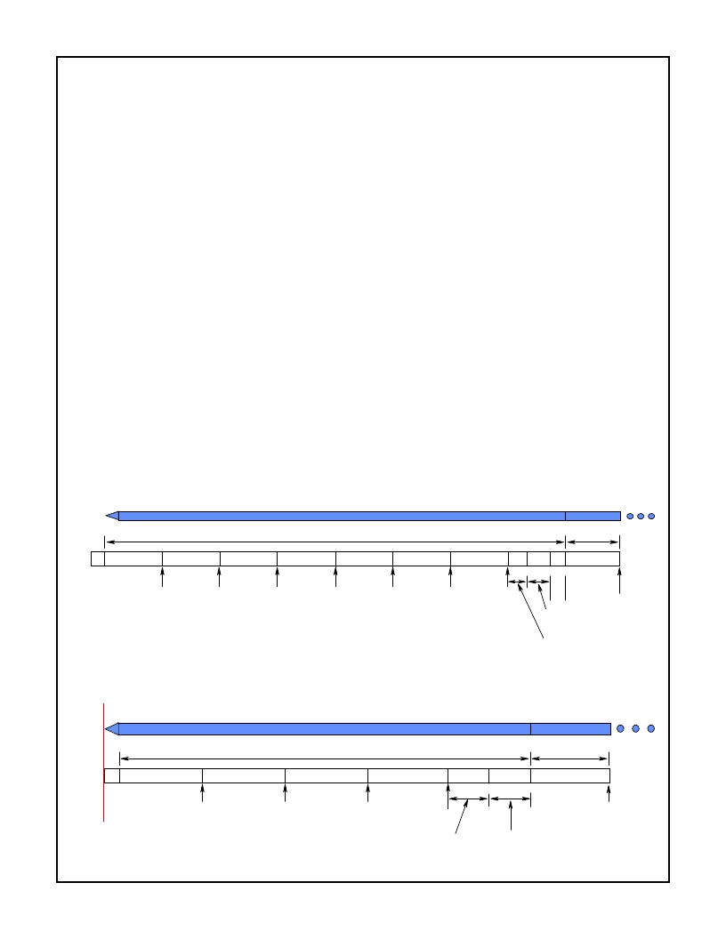
A projected worst case time line for the acquisition of a signal
in the two antenna case is shown in Figure 15. The synchroni-
zation part of the preamble is 128 symbols long followed by a
16-bit SFD. The receiver must scan the two antennas to deter-
mine if a signal is present on either one and, if so, which has
the better signal. The timeline is broken into 16 symbol blocks
(dwells) for the scanning process. This length of time is neces-
sary to allow enough integration of the signal to make a good
NOTES:
1. Worst Case Timing; antenna dwell starts before signal is full strength.
2. Time line shown assumes that antenna 2 gets insufficient signal.
FIGURE 15. DUAL ANTENNA ACQUISITION TIMELINE
FIGURE 16. SINGLE ANTENNA ACQUISITION TIMELINE
16 SYMBOLS
A1
126 SYMBOL SYNC
SFD
JUST
MISSED
DET
ANT1
SYMB
TIMING
DETECT
ANT1
CHECK
ANT2
TX
POWER
RAMP
NO
SIG
FOUND
ANT2
16 SYMBOLS 16 SYMBOLS 16 SYMBOLS 16 SYMBOLS 16 SYMBOLS 16 SYMBOLS
A2
A1
A2
7S
A1
16 SYMBOLS
A1
A1
A2
A1
A1
DETECT
ANT1
SFD DET
START DATA
SEED
DESCRAMBLER
7S
CHECK
ANT2
INTERNAL
SET UP TIME
VERIFY
ANT1
2
2
16 SYMBOLS
78 SYMBOL SYNC
SFD
JUST
MISSED
DET
DETECT
TX
POWER
RAMP
16 SYMBOLS
16 SYMBOLS
16 SYMBOLS
7 SYM
16 SYMBOLS
SYMB
TIMING
VERIFY
SFD DET
START DATA
SEED
DESCRAMBLER
7 SYM
INTERNAL
SET UP TIME
相關(guān)PDF資料 |
PDF描述 |
|---|---|
| HSR101 | Silicon Schottky Barrier Diode for Various detector, High speed switching(用于多種檢波和高速開關(guān)的肖特基勢壘二極管) |
| HSRD1056RH165S | Converter IC |
| HSRD1056RH169H | Converter IC |
| HSRD1056RH169S | Converter IC |
| HSRD1056RH240H | Converter IC |
相關(guān)代理商/技術(shù)參數(shù) |
參數(shù)描述 |
|---|---|
| HSP3824VI96S5001 | 制造商:Harris Corporation 功能描述: |
| HSP40223221 | 制造商:PARMAR 功能描述:BALLAST HPS/MH 400W 制造商:PARMAR 功能描述:BALLAST, HPS/MH, 400W |
| HSP4070C | 制造商:JLWORLD 制造商全稱:JLWORLD 功能描述:SPEAKER SOUND GENERATORS |
| HSP40G-8 | 制造商:JLWORLD 制造商全稱:JLWORLD 功能描述:SPEAKER SOUND GENERATORS |
| HSP43124 | 制造商:INTERSIL 制造商全稱:Intersil Corporation 功能描述:Serial I/O Filter |
發(fā)布緊急采購,3分鐘左右您將得到回復(fù)。