- 您現(xiàn)在的位置:買賣IC網(wǎng) > PDF目錄224506 > MT48LC32M4A2P-7ELIT:G 32M X 4 SYNCHRONOUS DRAM, 5.4 ns, PDSO54 PDF資料下載
參數(shù)資料
| 型號: | MT48LC32M4A2P-7ELIT:G |
| 元件分類: | DRAM |
| 英文描述: | 32M X 4 SYNCHRONOUS DRAM, 5.4 ns, PDSO54 |
| 封裝: | 0.400 INCH, LEAD FREE, PLASTIC, TSOP2-54 |
| 文件頁數(shù): | 11/74頁 |
| 文件大?。?/td> | 2385K |
第1頁第2頁第3頁第4頁第5頁第6頁第7頁第8頁第9頁第10頁當(dāng)前第11頁第12頁第13頁第14頁第15頁第16頁第17頁第18頁第19頁第20頁第21頁第22頁第23頁第24頁第25頁第26頁第27頁第28頁第29頁第30頁第31頁第32頁第33頁第34頁第35頁第36頁第37頁第38頁第39頁第40頁第41頁第42頁第43頁第44頁第45頁第46頁第47頁第48頁第49頁第50頁第51頁第52頁第53頁第54頁第55頁第56頁第57頁第58頁第59頁第60頁第61頁第62頁第63頁第64頁第65頁第66頁第67頁第68頁第69頁第70頁第71頁第72頁第73頁第74頁
PDF: 09005aef8091e66d/Source: 09005aef8091e625
Micron Technology, Inc., reserves the right to change products or specifications without notice.
128MSDRAM_2.fm - Rev. N 1/09 EN
19
1999 Micron Technology, Inc. All rights reserved.
128Mb: x4, x8, x16 SDRAM
Functional Description
Notes:
1. For full-page accesses: y = 2,048 (x4), y = 1,024 (x8), and y = 512 (x16).
2. For BL = 2, A1–A9, A11 (x4), A1–A9 (x8), or A1–A8 (x16) select the block-of-two burst; A0
selects the starting column within the block.
3. For BL = 4, A2–A9, A11 (x4), A2–A9 (x8), or A2–A8 (x16) select the block-of-four burst; A0–
A1 select the starting column within the block.
4. For BL = 8, A3–A9, A11 (x4), A3–A9 (x8), or A3–A8 (x16) select the block-of-eight burst; A0–
A2 select the starting column within the block.
5. For a full-page burst, the full row is selected and A0–A9, A11 (x4), A0–A9 (x8), or A0–A8
(x16) select the starting column.
6. Whenever a boundary of the block is reached within a given sequence above, the following
access wraps within the block.
CAS Latency
The CL is the delay, in clock cycles, between the registration of a READ command and
the availability of the first piece of output data. The latency can be set to 2 or 3 clocks.
If a READ command is registered at clock edge n and the latency is m clocks, the data will
be available by clock edge n + m. The DQ will start driving as a result of the clock edge 1
cycle earlier (n + m - 1), and provided that the relevant access times are met, the data will
be valid by clock edge n + m. For example, assuming that the clock cycle time is such that
all relevant access times are met, if a read command is registered at T0 and the latency is
programmed to 2 clocks, the DQ will start driving after T1 and the data will be valid by
T2, as shown in Figure 8 on page 20. Table 6 on page 20 indicates the operating frequen-
cies at which each CL setting can be used.
Reserved states should not be used as unknown operation or incompatibility with future
versions may result.
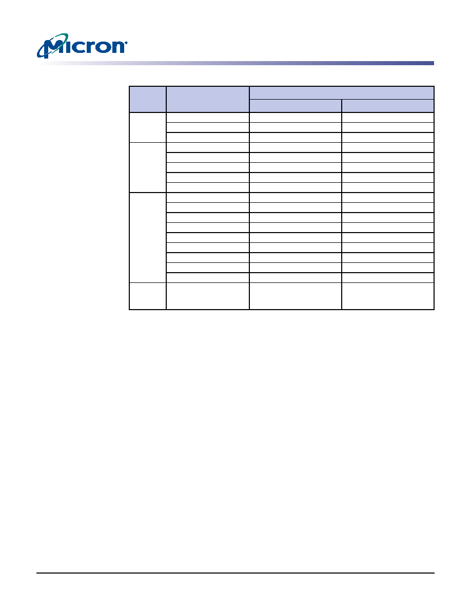
Table 5:
Burst Definition
Burst
Length
Starting Column
Address
Order of Accesses Within a Burst
Type = Sequential
Type = Interleaved
2
A0
00-1
0-1
11-0
1-0
4
A1
A0
0
0-1-2-3
0
1
1-2-3-0
1-0-3-2
1
0
2-3-0-1
1
3-0-1-2
3-2-1-0
8
A2
A1
A0
0
0-1-2-3-4-5-6-7
0
1
1-2-3-4-5-6-7-0
1-0-3-2-5-4-7-6
0
1
0
2-3-4-5-6-7-0-1
2-3-0-1-6-7-4-5
0
1
3-4-5-6-7-0-1-2
3-2-1-0-7-6-5-4
1
0
4-5-6-7-0-1-2-3
1
0
1
5-6-7-0-1-2-3-4
5-4-7-6-1-0-3-2
1
0
6-7-0-1-2-3-4-5
6-7-4-5-2-3-0-1
1
7-0-1-2-3-4-5-6
7-6-5-4-3-2-1-0
Full page
(y)
n = A0–A11/9/8
(location 0–y)
Cn, Cn + 1, Cn + 2,
Cn + 3, Cn + 4...,
...Cn - 1, Cn
Not supported
相關(guān)PDF資料 |
PDF描述 |
|---|---|
| MT55L256L18FT-12TR | 256K X 18 ZBT SRAM, 9 ns, PQFP100 |
| MT55L256L32FT-12 | 256K X 32 ZBT SRAM, 9 ns, PQFP100 |
| MT55L512V18PF-6 | 512K X 18 ZBT SRAM, 3.5 ns, PBGA165 |
| MT57W4MH9CF-6 | 4M X 9 DDR SRAM, 0.5 ns, PBGA165 |
| MT58L128L36D1T-5IT | 128K X 36 STANDARD SRAM, 2.8 ns, PQFP100 |
相關(guān)代理商/技術(shù)參數(shù) |
參數(shù)描述 |
|---|---|
| MT48LC32M4A2TG | 制造商:MICRON 制造商全稱:Micron Technology 功能描述:SYNCHRONOUS DRAM |
| MT48LC32M4A2TG-75 | 制造商:MICRON 制造商全稱:Micron Technology 功能描述:SYNCHRONOUS DRAM |
| MT48LC32M4A2TG-75IT | 制造商:MICRON 制造商全稱:Micron Technology 功能描述:SYNCHRONOUS DRAM |
發(fā)布緊急采購,3分鐘左右您將得到回復(fù)。