- 您現(xiàn)在的位置:買賣IC網(wǎng) > PDF目錄224506 > MT48LC32M4A2P-7ELIT:G 32M X 4 SYNCHRONOUS DRAM, 5.4 ns, PDSO54 PDF資料下載
參數(shù)資料
| 型號: | MT48LC32M4A2P-7ELIT:G |
| 元件分類: | DRAM |
| 英文描述: | 32M X 4 SYNCHRONOUS DRAM, 5.4 ns, PDSO54 |
| 封裝: | 0.400 INCH, LEAD FREE, PLASTIC, TSOP2-54 |
| 文件頁數(shù): | 47/74頁 |
| 文件大小: | 2385K |
第1頁第2頁第3頁第4頁第5頁第6頁第7頁第8頁第9頁第10頁第11頁第12頁第13頁第14頁第15頁第16頁第17頁第18頁第19頁第20頁第21頁第22頁第23頁第24頁第25頁第26頁第27頁第28頁第29頁第30頁第31頁第32頁第33頁第34頁第35頁第36頁第37頁第38頁第39頁第40頁第41頁第42頁第43頁第44頁第45頁第46頁當前第47頁第48頁第49頁第50頁第51頁第52頁第53頁第54頁第55頁第56頁第57頁第58頁第59頁第60頁第61頁第62頁第63頁第64頁第65頁第66頁第67頁第68頁第69頁第70頁第71頁第72頁第73頁第74頁
PDF: 09005aef8091e66d/Source: 09005aef8091e625
Micron Technology, Inc., reserves the right to change products or specifications without notice.
128MSDRAM_2.fm - Rev. N 1/09 EN
51
1999 Micron Technology, Inc. All rights reserved.
128Mb: x4, x8, x16 SDRAM
Notes
1. All voltages referenced to VSS.
2. This parameter is sampled. VDD, VDDQ = +3.3V; f = 1 MHz, TA = 25°C; pin under test
biased at 1.4V.
3. IDD is dependent on output loading and cycle rates. Specified values are obtained
with minimum cycle time and the outputs open.
4. Enables on-chip refresh and address counters.
5. The minimum specifications are used only to indicate cycle time at which proper
operation over the full temperature range (0°C ≤ TA ≤ +70°C (commercial), –40°C ≤ TA ≤
+85°C (industrial), and –40°C ≤ TA ≤ +105°C (automotive) ) is ensured.
6. An initial pause of 100s is required after power-up, followed by two AUTO REFRESH
commands, before proper device operation is ensured. (VDD and VDDQ must be pow-
ered up simultaneously. VSS and VSSQ must be at same potential.) The two AUTO
REFRESH command wake-ups should be repeated any time the tREF refresh require-
ment is exceeded.
7. AC characteristics assume tT = 1ns.
8. In addition to meeting the transition rate specification, the clock and CKE must tran-
sit between VIH and VIL (or between VIL and VIH) in a monotonic manner.
9. Outputs measured at 1.5V with equivalent load:
Q
50pF
10. tHZ defines the time at which the output achieves the open circuit condition; it is not
a reference to VOH or VOL. The last valid data element will meet tOH before going
High-Z.
11. AC timing and IDD tests have VIL = 0V and VIH = 3V, with timing referenced to 1.5V
crossover point. If the input transition time is longer than 1 ns, then the timing is ref-
erenced at VIL (MAX) and VIH (MIN) and no longer at the 1.5V crossover point. CLK
should always be 1.5V referenced to crossover. Refer to Micron technical note
TN-48-09 for more details.
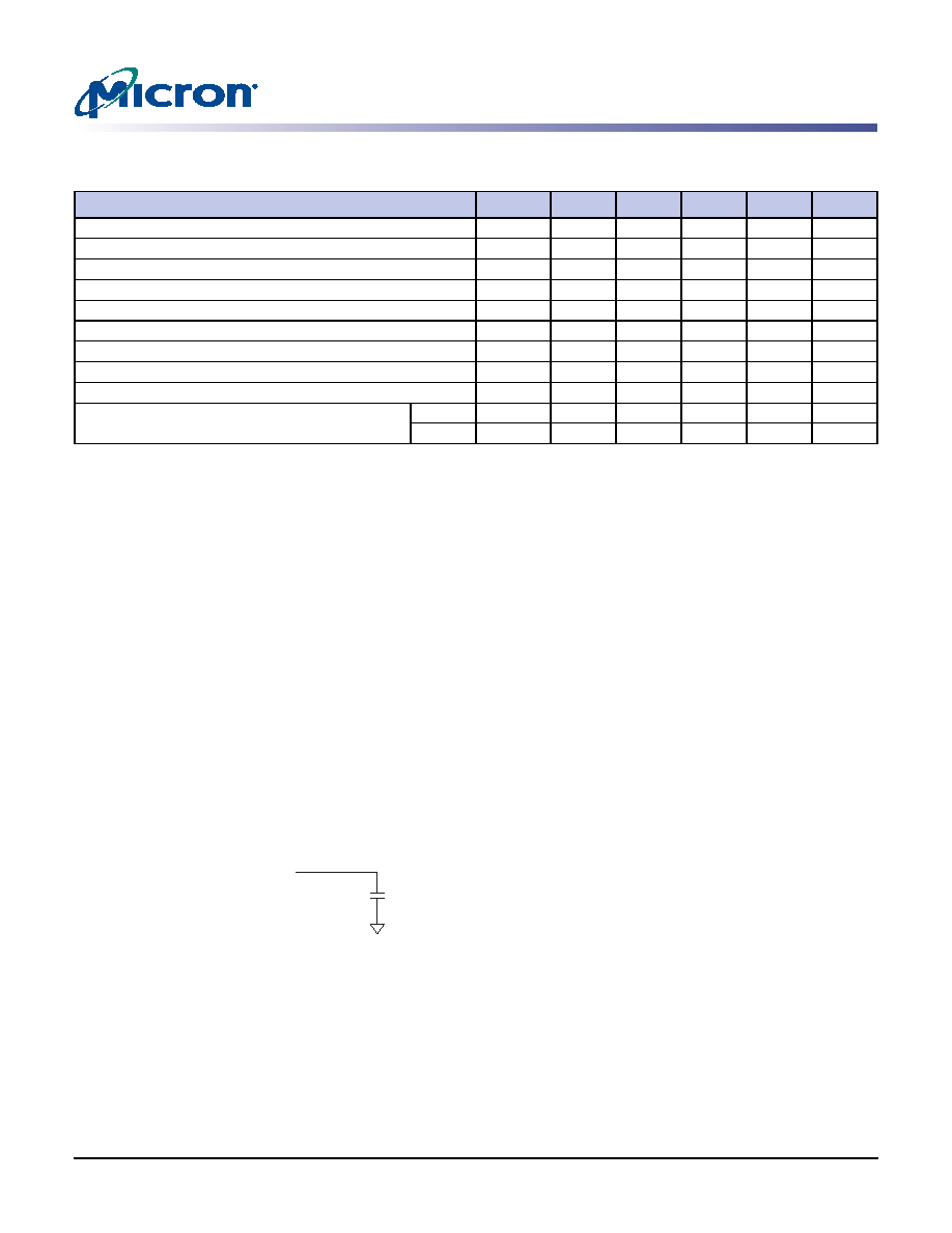
DQM to data mask during WRITEs
tDQM
000
tCK
DQM to data High-Z during READs
tDQZ
222
tCK
WRITE command to input data delay
tDWD
000
tCK
Data-in to ACTIVE command
tDAL
5
4
5
tCK
Data-in to PRECHARGE command
tDPL
222
tCK
Last data-in to burst STOP command
tBDL
111
tCK
Last data-in to new READ/WRITE command
tCDL
111
tCK
Last data-in to PRECHARGE command
tRDL
222
tCK
LMR command to ACTIVE or REFRESH command
tMRD
222
tCK
Data-out to High-Z from PRECHARGE command
CL = 3
tROH(3)
333
tCK
CL = 2
tROH(2)
–
2
tCK
Table 18:
AC Functional Characteristics
Notes: 5, 6, 7, 8, 9, 11; notes appear on page 51
Parameter
Symbol
-6A
-7E
-75
Units
Notes
相關PDF資料 |
PDF描述 |
|---|---|
| MT55L256L18FT-12TR | 256K X 18 ZBT SRAM, 9 ns, PQFP100 |
| MT55L256L32FT-12 | 256K X 32 ZBT SRAM, 9 ns, PQFP100 |
| MT55L512V18PF-6 | 512K X 18 ZBT SRAM, 3.5 ns, PBGA165 |
| MT57W4MH9CF-6 | 4M X 9 DDR SRAM, 0.5 ns, PBGA165 |
| MT58L128L36D1T-5IT | 128K X 36 STANDARD SRAM, 2.8 ns, PQFP100 |
相關代理商/技術參數(shù) |
參數(shù)描述 |
|---|---|
| MT48LC32M4A2TG | 制造商:MICRON 制造商全稱:Micron Technology 功能描述:SYNCHRONOUS DRAM |
| MT48LC32M4A2TG-75 | 制造商:MICRON 制造商全稱:Micron Technology 功能描述:SYNCHRONOUS DRAM |
| MT48LC32M4A2TG-75IT | 制造商:MICRON 制造商全稱:Micron Technology 功能描述:SYNCHRONOUS DRAM |
發(fā)布緊急采購,3分鐘左右您將得到回復。